LTC4000
31
4000fb
For more information www.linear.com/LTC4000
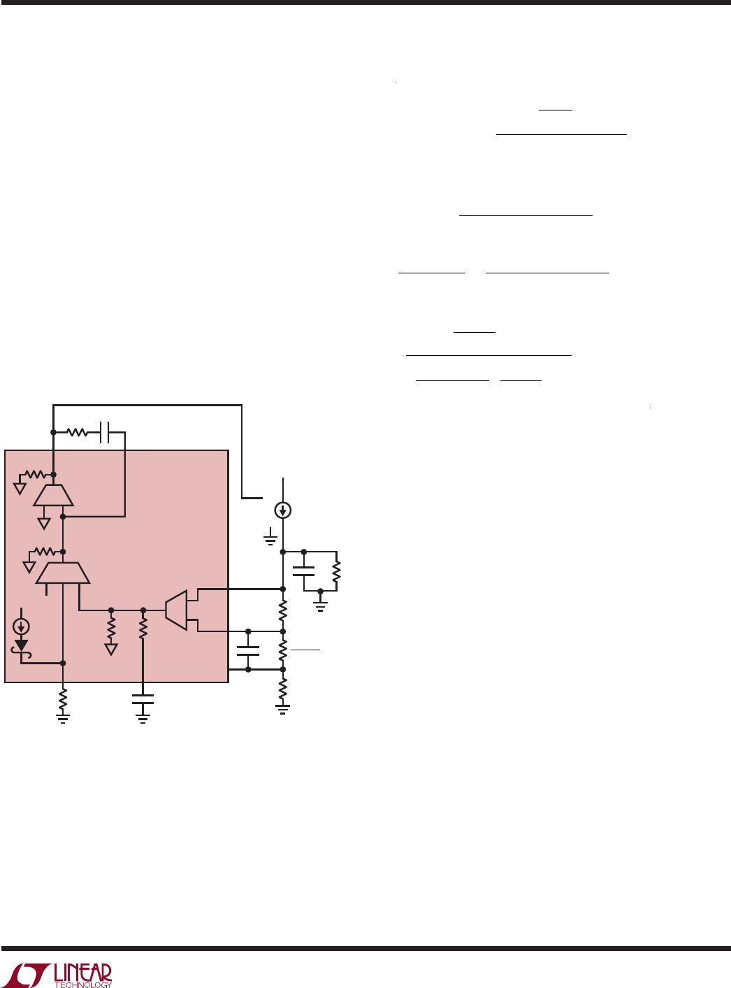
The Output Voltage Regulation Loop
The feedback signal for the output voltage regulation loop
is the voltage on the OFB pin, which is connected to the
center node of the resistor divider between the output
voltage (connected to C
SP
) and the FBG pin. This voltage
is compared to an internal reference (1.193V typical) by
the transconductance error amplifier A7. This amplifier
then drives the output transconductance amplifier (A10)
to appropriately adjust the voltage on the ITH pin driving
the external DC/DC converter to regulate the output volt-
age observed by the OFB pin. This loop is shown in detail
in Figure 21.
Figure 21. Simplified Linear Model of the Output Voltage
Regulation Loop
Figure 22. Simplified Linear Model of the Battery Float
Voltage Regulation Loop
The simplified loop transmission is as follows:
L
OV
(s) = g
m7
R
C
1
g
m10
C
C
s + 1
C
C
s
R
OFB2
R
OFB
R
L
R
L
C
L
s + 1
Gmo
p
(s)
where Gmo
p
(s) is the transfer function from V
ITH
to
the output current of the external DC/DC converter, and
R
OFB
= R
OFB1
+ R
OFB2
.
applicaTions inForMaTion
The Battery Float Voltage Regulation Loop
The battery float voltage regulation loop is very similar to
the output float voltage regulation loop. Instead of observ-
ing the voltage at the OFB pin, the battery float voltage
regulation loop observes the voltage at the BFB pin.
One significant difference is that while the value of R
L
in the output voltage loop can vary significantly, the
output resistance of the battery float voltage loop is a
small constant value approximately equal to the sum
of the on-resistance of the external PFET (R
DS(ON)
) and
the series internal resistance of the battery (R
BAT
). This
approximation is valid for any efficient system such that
most of the output power from the battery is delivered to
the system load and not dissipated on the battery inter-
nal resistance or the charging PFET on-resistance. For a
typical system, minimum R
L
is at least five times larger
than R
DS(ON)
+ R
BAT
and R
BFB
is at least 10
6
times larger
than R
BAT
. Figure 22 shows the detail of the battery float
voltage regulation loop.
CC
A7
g
m6
= 0.5m
A10
g
m10
= 0.1m
ITH
INPUT
BAT
INTERNALLY
PULLED HIGH
BFB
LTC4000
FBG
+
+
C
C
4000 F22
R
C
1.136V
R
BFB1
Gmo
p
(s)
R
BFB2
R
O6
R
O10
C
L
R
L
+
R
BAT
R
DS(ON)
R
CS
LOAD
CC
A7
g
m7
= 0.5m
A10
g
m10
= 0.1m
ITH
INPUT
LOAD
CSP
INTERNALLY
PULLED HIGH
OFB
LTC4000
FBG
+
+
C
C
4000 F21
R
C
1.193V
R
OFB1
Gmo
p
(s)
R
OFB2
R
O7
R
O10
C
L
R
L
+
LTC4000
32
4000fb
For more information www.linear.com/LTC4000
In Figure 22 the battery is approximated to be a signal
ground in series with the internal battery resistance R
BAT
.
Therefore, the simplified loop transmission is as follows:
L
BV
(s) = g
m6
R
C
1
g
m10
C
C
s + 1
C
C
s
R
BFB2
R
BFB
R
LB
R
LB
C
L
s + 1
Gmo
p
(s)
where Gmo
p
(s) is the transfer function from V
ITH
to
the output current of the external DC/DC converter,
R
BFB
= R
BFB1
+ R
BFB2
, and R
LB
= R
L
//(R
DS(ON)
+ R
CS
+
R
BAT
) represents the effective output resistance from the
LOAD node to GND.
The Battery Charge Current Regulation Loop
This final regulation loop combines certain dynamic char-
acteristics that are found in all the other three loops. The
feedback signal for this charge current regulation loop is
the sense voltage across the charge current sense resis-
tor (R
CS
). This voltage is amplified by a factor of 20 and
compared to the voltage on the CL pin by the transcon-
ductance error amplifier (A5). In a familiar fashion, this
amplifier drives the output transconductance amplifier
(A10) to appropriately adjust the voltage on the ITH pin
driving the external DC/DC converter to regulate the input
current across the sense resistor (R
CS
).
Due to the presence of the instant-on feature, description
of the charge current regulation loop has to be divided into
two separate operating regions. These regions of operation
depend on whether the voltage on the OFB pin is higher
or lower
than the instant-on threshold (V
OUT(INST_ON)
).
The Battery Charge Current Regulation Loop when
V
OFB
> V
OUT(INST_ON)
In this operating region, the external charging PFET’s gate
is driven low and clamped at V
BGATE(ON)
. The detail of this
loop is shown in Figure 23.
The simplified loop transmission is:
L
CC
(s) = g
m5
R
C
1
g
m10
C
C
s + 1
C
C
s
20R
CS
R2 C
IBMON
s + 1
( )
R1+R2
( )
C
IBMON
s + 1
R
L
R
f
+R
L
1
R
L
P R
f
( )
C
L
s + 1
Gmo
p
(s)
where Gmo
p
(s) is the transfer function from V
ITH
to the
output current of the external DC/DC converter, R
f
=
R
CS
+ R
DS(ON)
+ R
BAT
, and R
L
//R
f
represents the effective
resistance value resulting from the parallel combination
of R
L
and R
f
.
applicaTions inForMaTion
Figure 23. Simplified Linear Model of the Charge Current
Regulation Loop with the External Charging PFET Driven On
CC
A8
g
m8
= 0.33m
A10
g
m10
= 0.1m
ITH
INPUT
CSP
CSN
LTC4000
BAT
C
C
4000 F23
R
C
Gmo
p
(s)
R2
20k
R1
60k
R
O10
R
O5
+
C
L
R
L
C
IBMON
IBMONCL
+
R
BAT
R
DS(ON)
R
CS
1V
A5
g
m5
= 0.5m
R
CL
+
+
50µA/
5µA
BIAS
LTC4000
33
4000fb
For more information www.linear.com/LTC4000
The Battery Charge Current Regulation Loop when
V
OFB
is Regulated to V
OUT(INST_ON)
When the battery voltage is below the instant-on level,
the external charging PFET is driven linearly to regulate
the voltage at the output (connected to the CSP pin). The
output voltage is regulated such that the voltage at the OFB
pin is equal to the instant-on threshold (V
OUT(INST_ON)
).
If this external PFET regulation is fast compared to the
unity crossover frequency of the battery charge current
regulation loop, then the voltage at the output can be con-
sidered a small signal ground. However, in the LTC4000
the external PFET regulation is purposely made slow to
allow for a broader selection of possible PFETs to be used.
Therefore, the linear model of the PFET has to be included
in the analysis of the charge current regulation loop. The
detail of this loop is shown in Figure 24.
Figure 24. Simplified Linear Model of the Charge
Current Regulation Loop with the External Charging
PFET Linearly Regulated
The simplified loop transmission is:
L
CC2
(s) = g
m5
R
C
1
g
m10
C
C
s + 1
C
C
s
20R
CS
R2 C
IBMON
s + 1
( )
R1+R2
( )
C
IBMON
s + 1
R
L
R
fIDC
+R
L
1
R
L
P R
fIDC
( )
C
L
s + 1
C
g
g
mEXT
s + 1
R
CS
+R
BAT
R
fIDC
C
g
g
mEXT
s + 1
Gmo
p
(s)
where Gmo
p
(s) is the transfer function from V
ITH
to the
output current of the external DC/DC converter, g
mEXT
is
the small signal transconductance of the output PFET,
R
flDC
= R
CS
+ 1/g
mEXT
+ R
BAT
and R
L
//R
flDC
represents
the effective resistance value resulting from the parallel
combination of R
L
and R
flDC
.
applicaTions inForMaTion
CC
A8
g
m8
= 0.33m
A10
g
m10
= 0.1m
ITH
INPUT
CSP
CSN
LTC4000
BAT
C
C
4000 F24
R
C
Gmo
p
(s)
R2
20k
R1
60k
R
O10
R
O5
+
C
L
R
L
C
IBMON
IBMONCL
+
R
BAT
1
g
mEXT
R
CS
1V
A5
g
m5
= 0.5m
R
CL
+
+
50µA/
5µA
BIAS
C
g

LTC4000EGN#PBF

Mfr. #:
Manufacturer:
Analog Devices / Linear Technology
Description:
Battery Management High Voltage, High Current Controller for Battery Charging and Power Management
Lifecycle:
New from this manufacturer.
Delivery:
DHL FedEx Ups TNT EMS
Payment:
T/T Paypal Visa MoneyGram Western Union