LTC4000
22
4000fb
For more information www.linear.com/LTC4000
applicaTions inForMaTion
The value of R3 and R
D
can now be set according to the
following formula:
R3 =
R
NTC
at cold_ threshold R
NTC
at hot_ threshold
2.461
R
D
= 0.219 R
NTC
at cold_ threshold
1.219 R
NTC
at hot_ threshold
Note the important caveat that this method can only be
used to desensitize the thermal effect on the thermistor
and hence push the hot and cold temperature thresholds
apart from each other. When using the formulas above,
if the user finds that a negative value is needed for R
D
,
the two temperature thresholds selected are too close to
each other and a higher sensitivity thermistor is needed.
For example, this method can be used to set the hot
and cold thresholds independently to 60°C and –5°C.
Using a Vishay Curve 2 thermistor whose nominal value
at 25°C is 100k, the formula results in R3 = 130k and
R
D
= 41.2k for the closest 1% resistors values.
To increase thermal sensitivity such that the valid charging
temperature band is much smaller than 40°C, it is pos-
sible to put a PTC (positive thermal coefficient) resistor
in series with R3 between the BIAS pin and the NTC pin.
This PTC resistor also needs to be thermally coupled with
the battery. Note that this method increases
the number of
thermal sensing connections to the battery pack from one
wire to three wires. The exact value of the nominal PTC
resistor required can be calculated using a similar method
as described above, keeping in mind that the threshold at
the NTC pin is always 75% and 35% of V
BIAS
.
Leaving the NTC pin floating or connecting it to a capacitor
disables all NTC functionality.
The F LT and CHRG Indicator Pins
The F LT and CHRG pins in the LTC4000 provide status
indicators. Table 2 summarizes the mapping of the pin
states to the part status.
Table 2. F LT and CHRG Status Indicator
F LT CHRG STATUS
0 0 NTC Over Ranged – Charging Paused
1 0 Charging Normally
0 1 Charging Terminated and Bad Battery Detected
1 1 V
IBMON
< (V
C/X
– 10mV)
where 1 indicates a high impedance state and 0 indicates
a low impedance pull-down state.
Note that V
IBMON
< (V
CX
– 10mV) corresponds to charge
termination only if the C/X termination is selected. If the
charger timer termination is selected, constant voltage
charging may continue for the remaining charger timer
period even after the indicator pins indicate that V
IBMON
< (V
CX
– 10mV). This is also true when no termination is
selected, constant voltage charging will continue even after
the indicator pins indicate that V
IBMON
< (V
CX
– 10mV).
The BIAS Pin
For ease of use the LTC4000 provides a low dropout volt-
age regulator output on the BIAS pin. Designed to provide
up to 0.5mA of current at 2.9V, this pin requires at least
470nF of low ESR bypass capacitance for stability.
Use the BIAS pin as the pull-up source for the NTC resis-
tor networks, since the internal reference for the NTC
circuitry is based on a ratio of the voltage on the BIAS
pin. Furthermore, various 100k pull-up resistors
can be
conveniently connected to the BIAS pin.
LTC4000
23
4000fb
For more information www.linear.com/LTC4000
applicaTions inForMaTion
Figure 11. Error Amplifier Followed by Output Amplifier Driving
CC and ITH Pins
Setting the Input Voltage Monitoring Resistor Divider
The falling threshold voltage level for this monitoring
function can be calculated as follows:
R
VM1
=
V
VM _RST
1.193V
1
R
VM2
where R
VM1
and R
VM2
form a resistor divider connected
between the monitored voltage and GND, with the center
tap point connected to the VM pin as shown in Figure 6. The
rising threshold voltage level can be calculated similarly.
Compensation
In order for the LTC4000 to control the external DC/DC
converter, it has to be able to overcome the sourcing bias
current of the ITH or VC pin of the DC/DC converter. The
typical sinking capability of the LTC4000 at the ITH pin is
1mA at 0.4V with a maximum voltage range of 0V to 6V.
It is imperative that the local feedback of the DC/DC con-
verter be set up such that during regulation of any of the
LTC4000 loops this local loop is out of regulation and
sources as much current as possible from its ITH/VC pin.
For example for a DC/DC converter regulating its output
voltage, it is recommended that the converter feedback
divider is programmed to be greater than 110% of the
output voltage regulation level programmed at the OFB pin.
There are four feedback loops to consider when setting up
the compensation for the LTC4000.
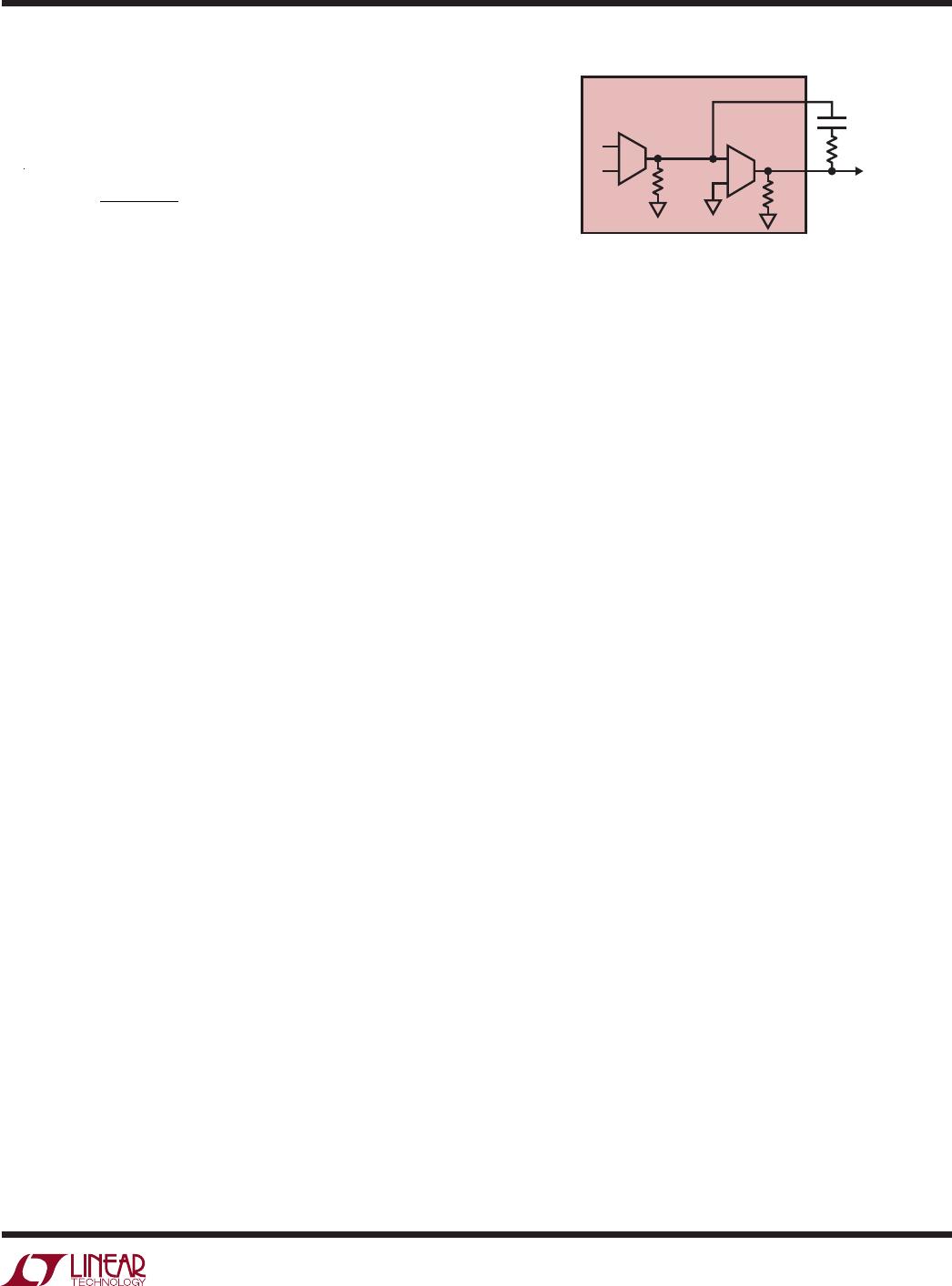
As mentioned
before
these loops are: the input current loop, the charge current
loop, the float voltage loop and the output voltage loop.
All of these loops have an error amp (A4-A7) followed by
another amplifier (A10) with the intermediate node driv-
ing the CC pin and the output of A10 driving the ITH pin
as shown in Figure 11. The most common compensation
network of a series capacitor (C
C
) and resistor (R
C
) between
the CC pin and the ITH pin is shown here.
Each of the loops has slightly different dynamics due to
differences in the feedback signal path. The analytic descrip-
tion of each of the loops is included in the Appendix sec-
tion. In most situations, an alternative empirical approach
to compensation, as described here, is more practical.
CC
ITH
LTC4000
+
C
C
4000 F11
R
C
A4-A7
g
m4-7
= 0.2m
A10
g
m10
= 0.1m
+
R
O4-7
R
O10
Empirical Loop Compensation
Based on the five analytical expressions given in the Ap-
pendix section, and the transfer function from the ITH
pin to the input and output current of the external DC/DC
converter, the user can analytically determine the complete
loop transfer function of each of the loops. Once these are
obtained, it is a matter of analyzing the gain and phase
bode plots to ensure that there is enough phase and gain
margin at unity crossover with the selected values of R
C
and C
C
for all operating conditions.
Even though it is clear that an analytical compensation
method is possible, sometimes certain complications
render this method difficult to tackle. These complica-
tions include the lack of easy availability of the switching
converter transfer function from the ITH or VC control
node to its input or output current, and the variability of
parameter values of the components such as the ESR of
the output capacitor or the R
DS(ON)
of the external PFETs.
Therefore a simpler and more practical way to compensate
the LTC4000 is provided here. This empirical method
involves injecting an AC signal into the loop, observing
the loop transient response and adjusting the
C
C
and R
C
values to quickly iterate towards the final values. Much
of the detail of this method is derived from Application
Note19 which can be found at www.linear.com using
AN19 in the search box.
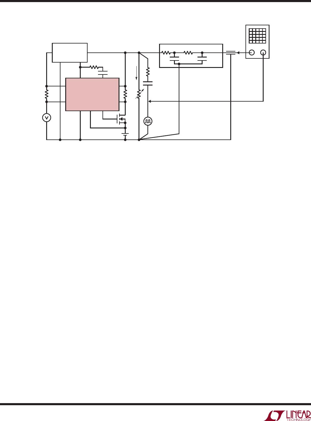
Figure 12 shows the recommended setup to inject an
AC-coupled output load variation into the loop. A function
generator with 50Ω output impedance is coupled through
a 50Ω/1000µF series RC network to the regulator output.
LTC4000
24
4000fb
For more information www.linear.com/LTC4000
Figure 12. Empirical Loop Compensation Setup
I
OUT
V
IN
CSN
CSP
IN
CLN
BATGND
LTC4000
50Ω
1W
50Ω
GENERATOR
f = 50Hz
R
C
ITHGND
SWITCHING
CONVERTER
4000 F12
BGATE
ITH CC
C
C
1000µF
(OBSERVE
POLARITY)
SCOPE
GROUND
CLIP
10k
A
1k
1500pF0.015µF
B
applicaTions inForMaTion
Generator frequency is set at 50Hz. Lower frequencies
may cause a blinking scope display and higher frequen-
cies may not allow sufficient settling time for the output
transient. Amplitude of the generator output is typically
set at 5V
P-P
to generate a 100mA
P-P
load variation. For
lightly loaded outputs (I
OUT
< 100mA), this level may be
too high for small signal response. If the positive and
negative transition settling waveforms are significantly
different, amplitude should be reduced. Actual amplitude
is not particularly important because it is the shape of
the resulting regulator output waveform which indicates
loop stability.
A 2-pole oscilloscope filter with f = 10kHz is used to
block switching frequencies. Regulators without added
LC output filters have switching frequency signals at their
outputs which may be much higher amplitude than the
low frequency settling waveform to be studied. The filter
frequency is high enough for most applications to pass
the settling waveform with no distortion.
Oscilloscope and generator connections should be made
exactly as shown in Figure 12 to prevent ground loop er-
rors. The oscilloscope is synced by connecting the chan-
nelB probe to the generator output, with the ground clip
of the second probe
connected to
exactly the same place
as channel A ground. The standard 50Ω BNC sync output
of the generator should not be used because of ground
loop errors. It may also be necessary to isolate either
the generator or oscilloscope from its third wire (earth
ground) connection in the power plug to prevent ground
loop errors in the scope display. These ground loop errors
are checked by connecting channel A probe tip to exactly
the same point as the probe ground clip. Any reading on
channel A indicates a ground loop problem.
Once the proper setup is made, finding the optimum
values for the frequency compensation network is fairly
straightforward. Initially, C
C
is made large (≥1μF) and R
C
is made small (≈10k). This nearly always ensures that the
regulator will be stable enough to start iteration. Now, if
the regulator output waveform is single-pole over damped
(see the waveforms in Figure 13), the value of C
C
is re-
duced in steps of about 2:1 until the response becomes
slightly under damped. Next, R
C
is increased in steps of
2:1 to introduce a loop zero. This will normally improve
damping and allow the value of C
C
to be further reduced.
Shifting back and forth between R
C
and C
C
variations will
allow one to quickly find optimum values.

LTC4000EGN#PBF

Mfr. #:
Manufacturer:
Analog Devices / Linear Technology
Description:
Battery Management High Voltage, High Current Controller for Battery Charging and Power Management
Lifecycle:
New from this manufacturer.
Delivery:
DHL FedEx Ups TNT EMS
Payment:
T/T Paypal Visa MoneyGram Western Union