LTC4000
25
4000fb
For more information www.linear.com/LTC4000
If the regulator response is under damped with the initial
large value of C
C
, R
C
should be increased immediately before
larger values of C
C
are tried. This will normally bring about
the over damped starting condition for further iteration.
The optimum values for R
C
and C
C
normally means the
smallest value for C
C
and the largest value for R
C
which
still guarantee well damped response, and which result in
the largest loop bandwidth and hence loop settling that is
as rapid as possible. The reason for this approach is that
it minimizes the variations in output voltage caused by
input ripple voltage and output load transients.
A switching regulator which is grossly over damped will
never oscillate, but it may have unacceptably large output
transients following sudden changes in input voltage or
output loading. It may also suffer from excessive overshoot
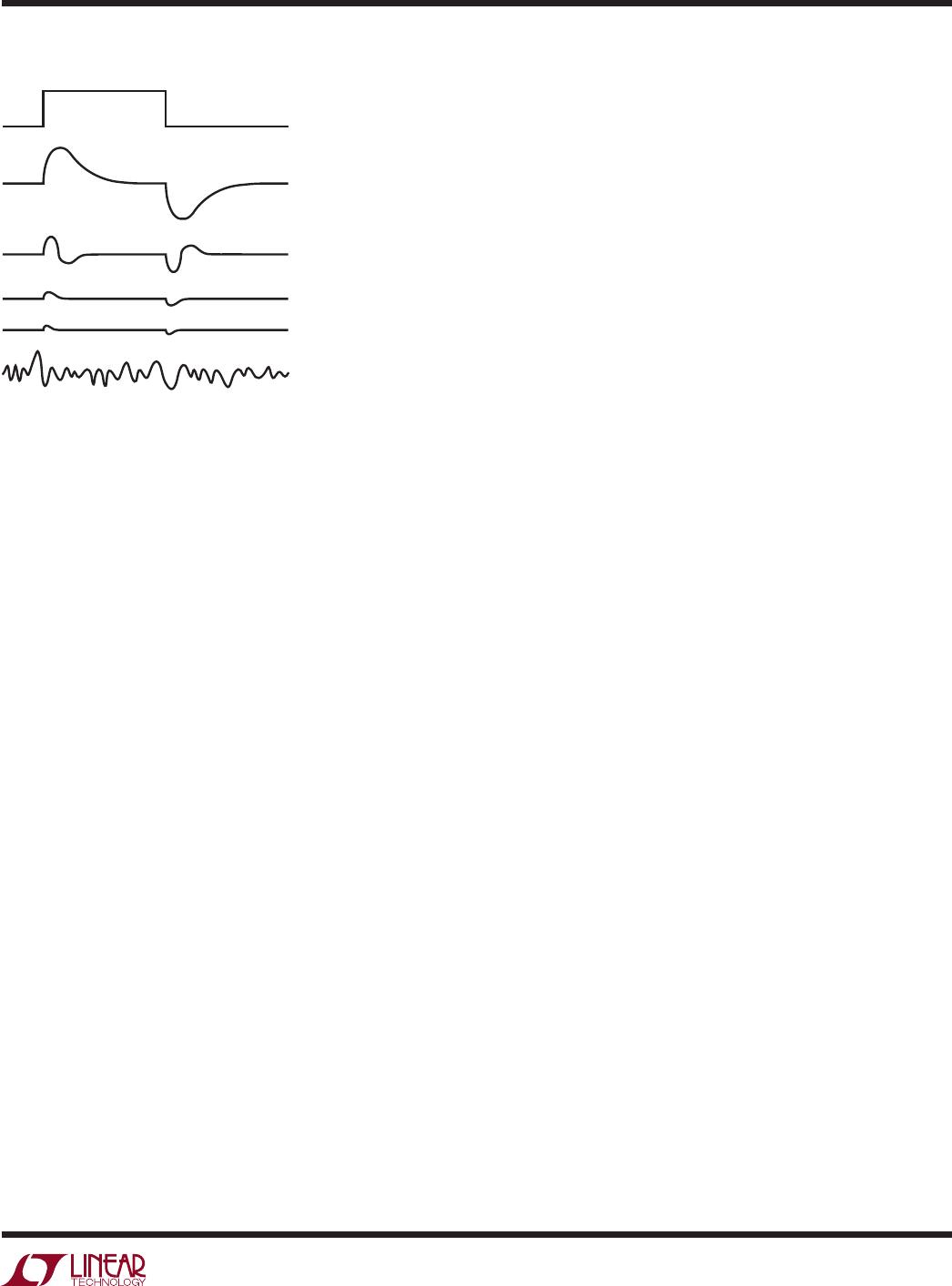
Figure 13. Typical Output Transient Response at Various
Stability Level
GENERATOR OUTPUT
REGULATOR OUTPUT
WITH LARGE C
C
, SMALL R
C
WITH REDUCED C
C
, SMALL R
C
FURTHER REDUCTION IN C
C
MAY BE POSSIBLE
IMPROPER VALUES WILL
CAUSE OSCILLATIONS
EFFECT OF INCREASED R
C
4000 F13
applicaTions inForMaTion
problems on startup or short circuit recovery. To guarantee
acceptable loop stability under all conditions, the initial
values chosen for R
C
and C
C
should be checked under all
conditions of input voltage and load current. The simplest
way of accomplishing this is to apply load currents of
minimum, maximum and several points in between. At
each load current, input voltage is varied from minimum
to maximum while observing the settling waveform.
If large temperature variations are expected for the system,
stability checks should also be done at the temperature
extremes. There can be significant temperature varia-
tions in several key component parameters which affect
stability; in particular, input and output capacitor value
and their ESR, and inductor permeability. The external
converter parametric variations also need some consid-
eration especially the transfer function from the ITH/VC
pin voltage to the output variable (voltage or current). The
LTC4000 parameters that vary with temperature include
the transconductance and the output resistance of the
error amplifiers (A4-A7). For modest temperature varia-
tions, conservative over damping under worst-case room
temperature conditions is usually sufficient to guarantee
adequate stability at all temperatures.
One measure of stability margin is to vary
the selected
values of both R
C
and C
C
by 2:1 in all four possible com-
binations. If the regulator response remains reasonably
well damped under all conditions, the regulator can be
considered fairly tolerant of parametric variations. Any
tendency towards an under damped (ringing) response
indicates that a more conservative compensation may
be needed.
LTC4000
26
4000fb
For more information www.linear.com/LTC4000
applicaTions inForMaTion
DESIGN EXAMPLE
In this design example, the LTC4000 is paired with the
LT3845A buck converter to create a 10A, 3-cell LiFePO
4
battery charger. The circuit is shown on the front page
and is repeated here in Figure 14.
The input voltage monitor falling threshold is set at
14.3V according to the following formula:
R
VM1
=
14.3V
1.193V
1
100k 1.10M
The IL pin is left open such that the voltage on this pin
is >1.05V. The regulation voltage on the IIMON pin is
clamped at 1.0V with an accurate internal reference.
Therefore, the input current limit is set at 10A according
to the following formula:
R
IS
=
0.050V
10A
= 5m
R
CL
is set at 24.9such that the voltage at the CL pin
is 1.25V. Similar to the IIMON pin, the regulation voltage
on the IBMON pin is clamped at 1V with an accurate
internal reference. Therefore, the charge current limit
is set at 10A according to the following formula:
I
CLIM(MAX)
=
0.050V
R
CS
=
0.050V
5m
= 10A
The trickle charge current level is consequently set at
1.25A, according to the following formula:
I
CLIM(TRKL)
= 0.25µA
24.9k
5m
= 1.25A
The battery float voltage is set at 10.8V according to
the following formula:
R
BFB1
=
10.8
1.136
1
133k 1.13M
The bad battery detection time is set at 43 minutes
according to the following formula:
C
TMR
(nF) = t
BADBAT
(h) 138.5 =
43
60
138.5 = 100nF
Figure 14. 48V to 10.8V at 10A Buck Converter Charger for Three LiFePO
4
Cells
1.13M
14.7k
127k
10k
10k
3-CELL Li-Ion
BATTERY PACK
10.8V FLOAT
10A MAX CHARGE
CURRENT
NTHS0603
N02N1002J
1.15M
47nF
5mΩ
12V, 15A15V TO 60V
133k
CSN
CSP
BGATE
IGATE
BAT
OFB
FBG
BFB
NTC
CX
LTC4000
ITH CC IID
10M
5mΩ
LT3845A
100µF
OUT
V
C
SHDN
IN
RST
CLN
IN
ENC
CHRG
F LT
VM
IIMON
IBMON
22.1k
CLILTMR GND BIAS
22.1k
F
1.10M
100k
10nF
10nF
F0.1µF
4000 F14
Si7135DP
Si7135DP
3.0V
LTC4000
27
4000fb
For more information www.linear.com/LTC4000
applicaTions inForMaTion
The charge termination time is set at 2.9 hours accord-
ing to the following formula:
C
TMR
(nF)
=
t
TERMINATE
(h) 34.6
=
2.9 34.6
=
100nF
The C/X current termination level is programmed at 1A
according to the following formula:
R
CX
=
1A 5m
( )
+ 0.5mV
0.25µA
22.1k
Note that in this particular solution, the timer termina-
tion is selected since a capacitor connects to the TMR
pin. Therefore, this C/X current termination level only
applies to the CHRG indicator pin.
The output voltage regulation level is set at 12V accord-
ing to the following formula:
R
OFB1
=
12
1.193
1
127k 1.15M
The instant-on voltage level is consequently set at 9.79V
according to the following formula:
V
INST _ON
=
1150k
+
127k
127k
0.974V = 9.79V
The worst-case power dissipation during instant-on
operation can be calculated as follows:
During trickle charging:
P
TRKL
= 0.86 V
FLOAT
V
BAT
I
CLIM _ TRKL
= 0.86 10.8
[ ]
1A
= 9.3W
And beyond trickle charging:
P
INST _ON
= 0.86 V
FLOAT
V
BAT
I
CLIM
= 0.86 10.8 7.33
[ ]
10A
= 19.3W
Therefore, depending on the layout and heat sink avail-
able to the charging PMOS, the suggested PMOS over
temperature detection circuit included in Figure 7 may
need to be included. For the complete application circuit,
please refer to Figure 25.
The range of valid temperature for charging is set at
–1.5°C to 41.5°C by picking a 10k Vishay Curve 2 NTC
thermistor that is thermally coupled to the battery, and
connecting this in series with a regular 10k resistor to
the BIAS pin.
For compensation, the procedure described in the
empirical loop compensation section is followed. As
recommended, first aF C
C
and 10k R
C
is used, which
sets all the loops to be stable. For an example of typical
transient responses, the charge current regulation loop
when V
OFB
is regulated to V
OUT(INST_ON)
is used here.
Figure 15 shows the recommended setup to inject a
DC-coupled charge current variation into this particular
loop. The input to the CL pin is a square wave at 70Hz
with
the low level set at 120mV and the high level set
at
130mV, corresponding to a 1.2A and 1.3A charge
current (100mA charge current step). Therefore, in this
particular example the trickle charge current regulation
stability is examined. Note that the nominal trickle
charge current in this example is programmed at 1.25A
(R
CL
= 24.9kΩ).
Figure 15. Charge Current Regulation Loop Compensation Setup
LTC4000
10k 1k
4000 F15
0.015µF
SQUARE WAVE
GENERATOR
f = 60Hz
IBMON
CL
1500pF
B A

LTC4000EGN#PBF

Mfr. #:
Manufacturer:
Analog Devices / Linear Technology
Description:
Battery Management High Voltage, High Current Controller for Battery Charging and Power Management
Lifecycle:
New from this manufacturer.
Delivery:
DHL FedEx Ups TNT EMS
Payment:
T/T Paypal Visa MoneyGram Western Union