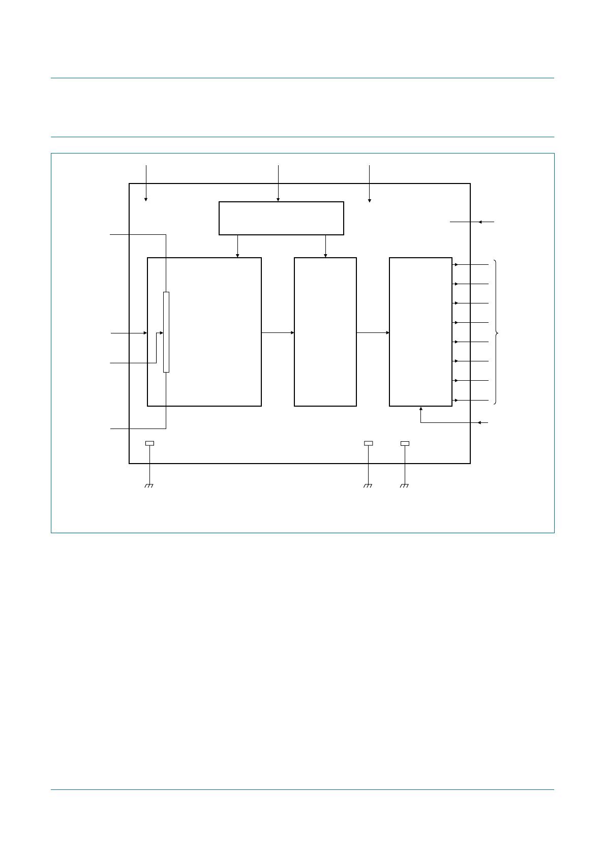
1. General description
The ADC0801S040 is an 8-bit universal analog-to-digital converter (ADC) for video and
general purpose applications. It converts the analog input signal from 2.7 V to 5.5 V into
8-bit binary-coded digital words at a maximum sampling rate of 40 MHz. All digital inputs
and outputs are CMOS/Transistor-Transistor Logic (TTL) compatible. A sleep mode allows
reduction of the device power consumption to 4 mW.
2. Features
n 8-bit resolution
n Operation between 2.7 V and 5.5 V
n Sampling rate up to 40 MHz
n DC sampling allowed
n High signal-to-noise ratio over a large analog input frequency range (7.3 effective bits
at 4.43 MHz full-scale input at f
clk
= 40 MHz)
n CMOS/TTL compatible digital inputs and outputs
n External reference voltage regulator
n Power dissipation only 30 mW (typical value)
n Low analog input capacitance, no buffer amplifier required
n Sleep mode (4 mW)
n No sample-and-hold circuit required
3. Applications
n Video data digitizing
n Camera
n Camcorder
n Radio communication
n Car alarm system
ADC0801S040
Single 8 bits ADC, up to 40 MHz
Rev. 02 — 18 August 2008 Product data sheet
ADC0801S040_2 © NXP B.V. 2008. All rights reserved.
Product data sheet Rev. 02 — 18 August 2008 2 of 19
NXP Semiconductors
ADC0801S040
Single 8 bits ADC, up to 40 MHz
4. Quick reference data
5. Ordering information
Table 1. Quick reference data
V
DDA
=V5toV6=3.3V;V
DDD
=V3toV4=3.3V;V
DDO
= V20 to V11 = 3.3 V; V
SSA
,V
SSD
and V
SSO
shorted together; V
i(a)(p-p)
= 1.84 V; C
L
= 20 pF; T
amb
= 0
°
C to 70
°
C; typical values measured at
T
amb
= 25
°
C unless otherwise specified.
Symbol Parameter Conditions Min Typ Max Unit
V
DDA
analog supply
voltage
2.7 3.3 5.5 V
V
DDD
digital supply
voltage
2.7 3.3 5.5 V
V
DDO
output supply
voltage
2.5 3.3 5.5 V
V
DD
supply voltage
difference
V
DDA
V
DDD
0.2 - +0.2 V
V
DDD
V
DDO
0.2 - +2.25 V
I
DDA
analog supply
current
- 46mA
I
DDD
digital supply
current
- 58mA
I
DDO
output supply
current
f
clk
= 40 MHz; ramp input;
C
L
=20pF
- 12mA
INL integral
non-linearity
ramp input; see
Figure 6 - ±0.5 ±0.75 LSB
DNL differential
non-linearity
ramp input; see
Figure 7 - ±0.25 ±0.5 LSB
f
clk(max)
maximum
clock
frequency
40 - - MHz
P
tot
total power
dissipation
V
DDA
=V
DDD
=V
DDO
= 3.3 V - 30 53 mW
Table 2. Ordering information
Type number Package
Name Description Version
ADC0801S040TS SSOP20 plastic shrink small outline package; 20 leads; body width 4.4 mm SOT266-1
ADC0801S040_2 © NXP B.V. 2008. All rights reserved.
Product data sheet Rev. 02 — 18 August 2008 3 of 19
NXP Semiconductors
ADC0801S040
Single 8 bits ADC, up to 40 MHz
6. Block diagram
Fig 1. Block diagram
7
9
R
lad
8
10
RB
RM
RT
VI
3
V
DDD
5
V
DDA
2
CMOS
OUTPUTS
LATCHES
CLOCK DRIVER
014aaa495
1
CLK
SLEEP
ADC0801S040
20
V
DDO
6
V
SSA
analog ground digital ground
4
V
SSD
11
V
SSO
output ground
analog
voltage input
data outputs
LSB
MSB
19 D7
18 D6
17 D5
16 D4
15 D3
14 D2
13 D1
12 D0
ANALOG - TO - DIGITAL
CONVERTER

ADC0801S040/DB

Mfr. #:
Manufacturer:
NXP Semiconductors
Description:
BOARD EVALUATION FOR ADC0801S040
Lifecycle:
New from this manufacturer.
Delivery:
DHL FedEx Ups TNT EMS
Payment:
T/T Paypal Visa MoneyGram Western Union

Products related to this Datasheet