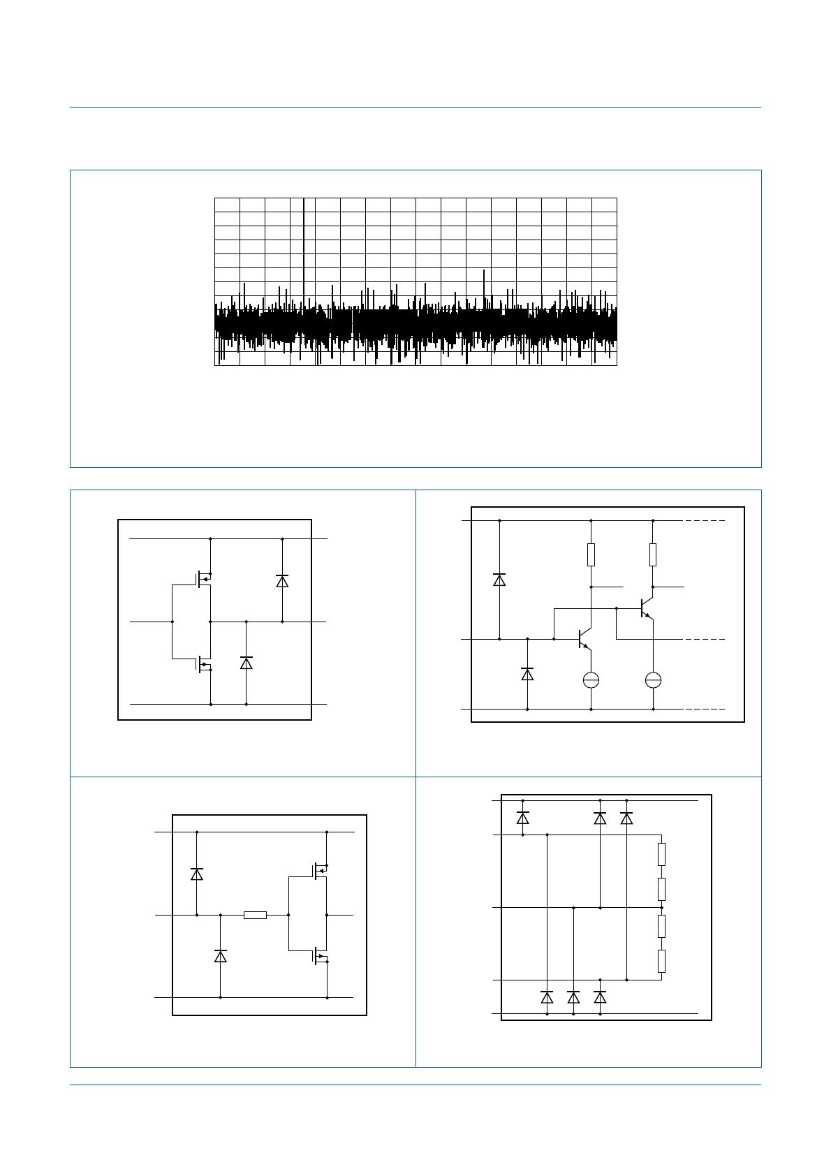
ADC0801S040_2 © NXP B.V. 2008. All rights reserved.
Product data sheet Rev. 02 — 18 August 2008 15 of 19
NXP Semiconductors
ADC0801S040
Single 8 bits ADC, up to 40 MHz
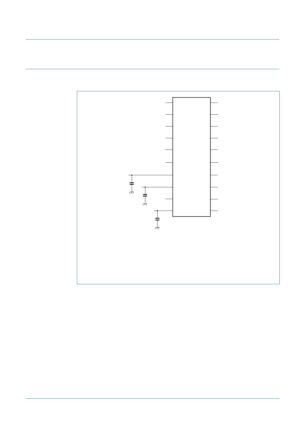
12. Application information
12.1 Application diagrams
The analog and digital supplies should be separated and decoupled.
The external voltage reference generator must be built in such a way that a good supply voltage
ripple rejection is achieved with respect to the LSB value. Eventually, the reference ladder voltages
can be derived from a well regulated V
DDA
supply through a resistor bridge and a decoupling
capacitor.
(1) RB, RM, RT are decoupled to V
SSA
.
Fig 15. Application diagram
100 nF
100 nF
100 nF
CLK
SLEEP
V
DDD
V
SSD
V
DDA
V
SSA
V
SSA
V
SSA
V
SSA
RB(1)
RM(1)
VI
RT(1)
V
DDO
D7
D6
D5
D4
D3
D2
D1
D0
V
SSO
1
2
3
4
5
6
7
8
9
10
11
12
20
19
18
17
16
15
14
13
ADC0801S040
014aaa500