ADC0801S040_2 © NXP B.V. 2008. All rights reserved.
Product data sheet Rev. 02 — 18 August 2008 8 of 19
NXP Semiconductors
ADC0801S040
Single 8 bits ADC, up to 40 MHz
[1] In addition to a good layout of the digital and analog ground, it is recommended that the rise and fall times of the clock must not be less
than 1 ns.
[2] Analog input voltages producing code 0 up to and including code 255:
a) V
offset
BOTTOM is the difference between the analog input which produces data equal to 00 and the reference voltage on pin RB
(V
RB
) at T
amb
= 25 °C.
b) V
offset
TOP is the difference between the reference voltage on pin RT (V
RT
) and the analog input which produces data outputs equal
to code 255 at T
amb
= 25 °C.
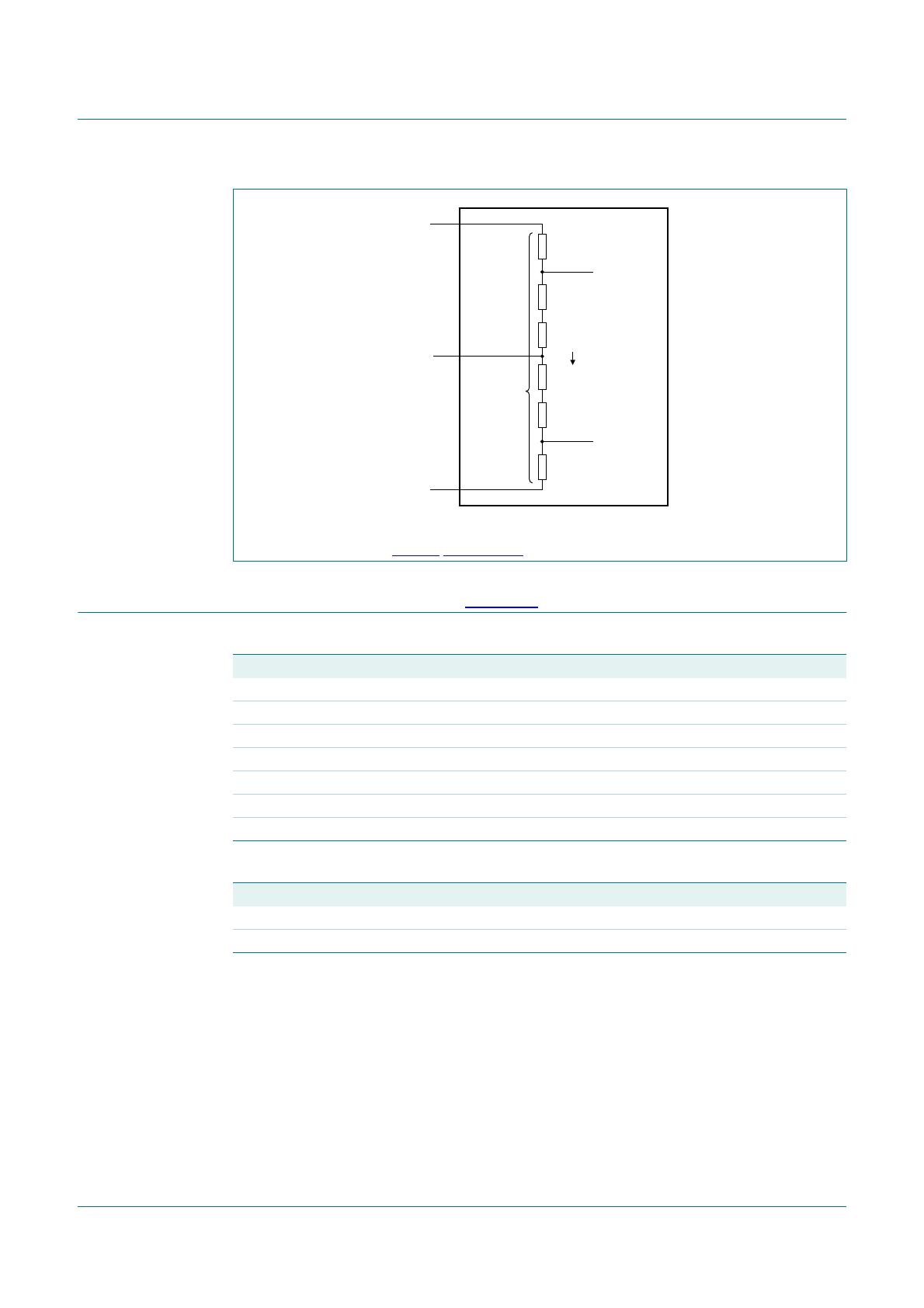
[3] To ensure the optimum linearity performance of such a converter architecture the lower and upper extremities of the converter reference
resistor ladder are connected to pins RB and RT via offset resistors R
OB
and R
OT
as shown in Figure 3.
a) The current flowing into the resistor ladder is and the full-scale input range at the converter, to cover code 0
to 255 is
b) Since R
L
, R
OB
and R
OT
have similar behavior with respect to process and temperature variation, the ratio
will be kept reasonably constant from device to device. Consequently variation of the output codes at a given input voltage depends
mainly on the difference V
RT
− V
RB
and its variation with temperature and supply voltage. When several ADCs are connected in
parallel and fed with the same reference source, the matching between each of them is optimized.
[4] The analog bandwidth is defined as the maximum input sine wave frequency which can be applied to the device. No glitches greater
than 2 LSB, nor any significant attenuation is observed in the reconstructed signal.
[5] The analog input settling time is the minimum time required for the input signal to be stabilized after a sharp full-scale input (square
wave signal) in order to sample the signal and obtain correct output data.
[6] Effective bits are obtained via a Fast Fourier Transform (FFT) treatment taking 8000 acquisition points per equivalent fundamental
period. The calculation takes into account all harmonics and noise up to half of the clock frequency (Nyquist frequency). Conversion to
signal-to-noise ratio: S/N = ENOB × 6.02 + 1.76 dB.
[7] Measurement carried out using video analyzer VM700A, where video analog signal is reconstructed through a DAC.
[8] Output data acquisition: the output data is available after the maximum delay time of t
d(o)
.
Differential phase
[7]
ϕ
dif
differential phase PAL modulated ramp - 0.25 - deg
Timing (f
clk
= 40 MHz; C
L
= 20 pF); see Figure 4
[8]
t
d(s)
sampling delay time - - 5 ns
t
h(o)
output hold time 5 - - ns
t
d(o)
output delay time V
DDO
= 4.75 V 8 12 15 ns
V
DDO
= 3.15 V 8 17 20 ns
V
DDO
= 2.7 V 8 18 21 ns
3-state output delay times; see
Figure 5
t
dHZ
active HIGH to float
delay time
-1418ns
t
dZL
float to active LOW delay
time
-1620ns
t
dZH
float to active HIGH
delay time
-1620ns
t
dLZ
active LOW to float delay
time
-1418ns
Table 6. Characteristics
…continued
V
DDA
=V5toV6=3.3V;V
DDD
=V3toV4=3.3V;V
DDO
= V20 to V11 = 3.3 V; V
SSA
,V
SSD
and V
SSO
shorted together; V
i(a)(p-p)
= 1.84 V; C
L
= 20 pF; T
amb
= 0
°
C to 70
°
C; typical values measured at T
amb
= 25
°
C unless otherwise specified.
Symbol Parameter Conditions Min Typ Max Unit
I
V
RT
V
RB
–
R
OB
R
L
R
OT
++
----------------------------------------
=
V
I
R
L
I
L
×
R
L
R
OB
R
L
R
OT
++
----------------------------------------
V
RT
V
RB
+()× 0.838 V
RT
V
RB
–()×== =
R
L
R
OB
R
L
R
OT
++
----------------------------------------