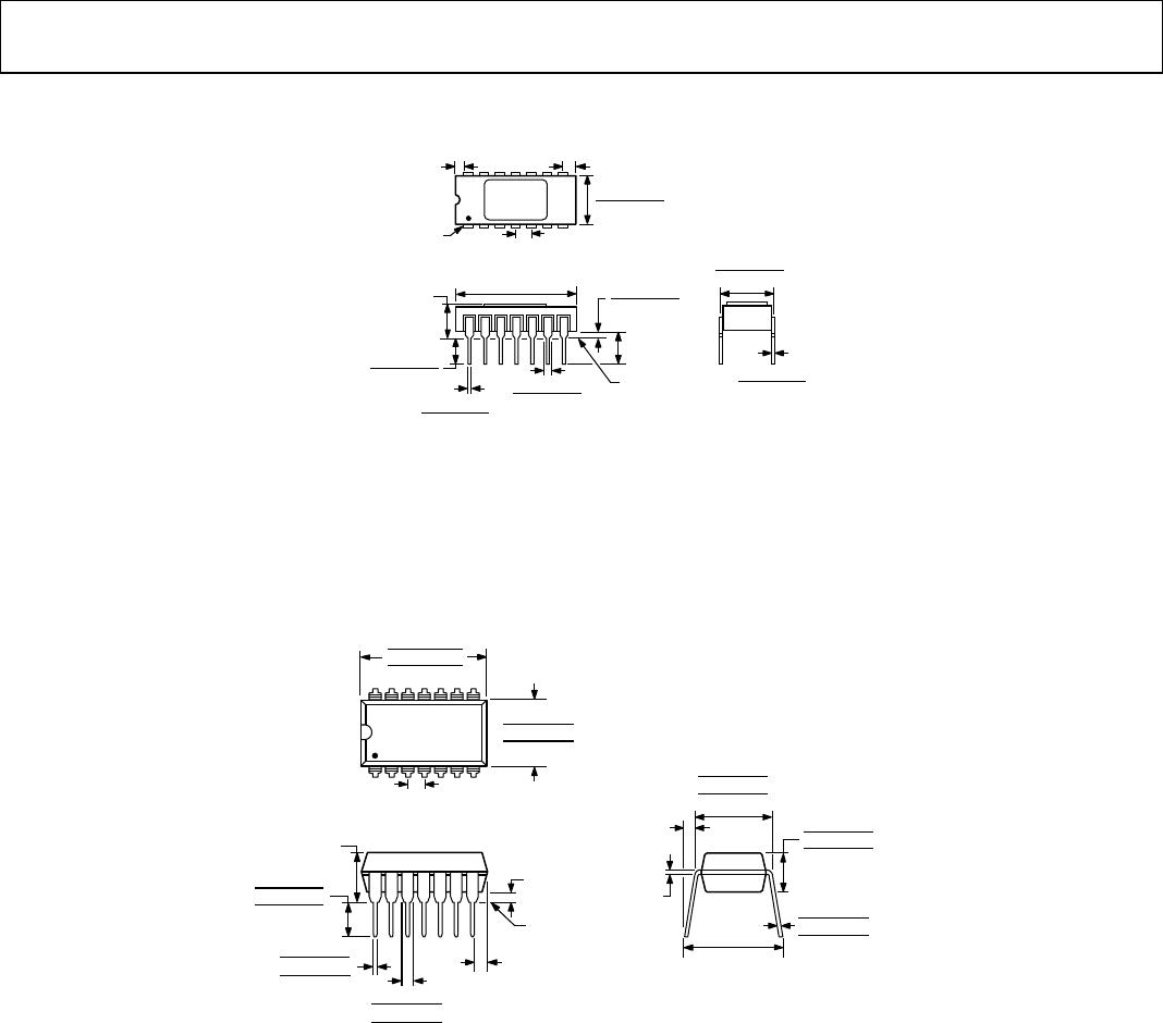
AD650 Data Sheet
Rev. E | Page 18 of 20
In signal recovery applications of a PLL, the desired output
signal is the voltage applied to the oscillator. In these situations,
a linear relationship between the input frequency and the
output voltage is desired; the AD650 makes a superb oscillator
for FM demodulation. The wide dynamic range and
outstanding linearity of the AD650 VFC allow simple
embodiment of high performance analog signal isolation or
telemetry systems. The circuit shown in Figure 22 uses a digital
phase detector that also provides proper feedback in the event
of unequal frequencies. Such phase-frequency detectors (PFDs)
are available in integrated form. For a full discussion of phase-
lock loop circuits see “Phase Lock Techniques,” 3
rd
Edition, by
F.M. Gardner, (John Wiley & Sons, Inc., 1979).
An analysis of this circuit must begin at the 7474 Dual D flip
flop. When the input carrier matches the output carrier in both
phase and frequency, the Q outputs of the flip flops rise at
exactly the same time. With two zeros, and then two ones on
the inputs of the exclusive or (XOR) gate, the output remains
low keeping the DMOS FET switched off. Also, the NAND gate
goes low resetting the flip-flops to zero. Throughout this entire
cycle, the DMOS integrator gate remains off, allowing the
voltage at the integrator output to remain unchanged from the
previous cycle. However, if the input carrier leads the output
carrier by a few degrees, the XOR gate is turned on for the short
time span that the two signals are mismatched. Because Q
2
is
low during the mismatch time, a negative current is fed into the
integrator, causing its output voltage to rise. This in turn
increases the frequency of the AD650 slightly, driving the
system towards synchronization. In a similar manner, if the
input carrier lags the output carrier, the integrator is forced
down slightly to synchronize the two signals.
Using a mathematical approach, the ±25 μA pulses from the
phase detector are incorporated into the phase-detector gain (K
d
).
radian/amperes104
2
μA25
6
×=
π
=
d
K
(9)
Also, the V/F converter is configured to produce 1 MHz in
response to a 10 V input so its gain (Ko) is
secvolt
radians
103.6
V10
Hz1012
5
6
×
×=
××π
=
O
K
(10)
The dynamics of the phase relationship between the input and
output signals can be characterized as a second order system
with natural frequency
n
).
C
KK
d
o
n
=ω
(11)
and damping factor ) is
2
d
o
KCKR
=ζ
(12)
For the values shown in Figure 22, these relations simplify to a
natural frequency of 35 kHz with a damping factor of 0.8.
For a simple approach to determine component values for other
PLL frequencies and VFC full-scale voltage, follow these steps:
1. Determine K
o
(in units of radians per volt second) from the
maximum input carrier frequency f
MAX
(in hertz) and the
maximum output voltage V
MAX
.
MAX
MAX
o
V
F
K
×π
=
2
(13)
2. Calculate a value for C based upon the desired loop
bandwidth f
n
. Note that this is the desired frequency range
of the output signal. The loop bandwidth (f
n
) is not the
maximum carrier frequency (f
MAX
). The signal can be very
narrow even though it is transmitted over a 1 MHz carrier.
secRad
101
7
2
×
×
××
=
F
V
f
K
C
n
o
(14)
where:
C units = farads
f
n
units = hertz
K
o
units = rad/volt × sec
3. Calculate R to yield a damping factor of approximately 0.8
using this equation:
VK
f
R
o
n
×
××=
Rad
105.2
6
(15)
where:
R units = ohms
f
n
units = hertz
K
o
units = rad/volt × sec
If in actual operation the PLL overshoots or hunts excessively
before reaching a final value, the damping factor can be raised
by increasing the value of R. Conversely, if the PLL is
overdamped, a smaller value of R should be used.
Data Sheet AD650
Rev. E | Page 19 of 20
OUTLINE DIMENSIONS
C
ONTROLLING DIMENSIONS ARE IN INCHES; MILLIMETER DIMENSIONS
(IN PARENTHESES) ARE ROUNDED-OFF INCH EQUIVALENTS FO
R
REFERENCE ONLY AND ARE NOT APPROPRIATE FOR USE IN DESIGN
.
14
1
7
8
0.310 (7.87)
0.220 (5.59)
PIN 1
0.080 (2.03) MAX
0.005 (0.13) MIN
SEATING
PLANE
0.023 (0.58)
0.014 (0.36)
0.060 (1.52)
0.015 (0.38)
0.200 (5.08)
MAX
0.200 (5.08)
0.125 (3.18)
0.070 (1.78)
0.030 (0.76)
0.100 (2.54)
BSC
0.150
(3.81)
MIN
0.765 (19.43) MAX
0.320 (8.13)
0.290 (7.37)
0.015 (0.38)
0.008 (0.20)
Figure 23. 14-Lead Side-Brazed Ceramic Dual In-Line Package [SBDIP]
(D-14)
Dimensions shown in inches and (millimeters)
COMPLIANT TO JEDEC STANDARDS MS-001
CONTROLLING DIMENSIONS ARE IN INCHES; MILLIMETER DIMENSIONS
(IN PARENTHESES) ARE ROUNDED-OFF INCH EQUIVALENTS FOR
REFERENCE ONLY AND ARE NOT APPROPRIATE FOR USE IN DESIGN.
CORNER LEADS MAY BE CONFIGURED AS WHOLE OR HALF LEADS.
070606-A
0.022 (0.56)
0.018 (0.46)
0.014 (0.36)
0.150 (3.81)
0.130 (3.30)
0.110 (2.79)
0.070 (1.78)
0.050 (1.27)
0.045 (1.14)
14
1
7
8
0.100 (2.54)
BSC
0.775 (19.69)
0.750 (19.05)
0.735 (18.67)
0.060 (1.52)
MAX
0.430 (10.92)
MAX
0.014 (0.36)
0.010 (0.25)
0.008 (0.20)
0.325 (8.26)
0.310 (7.87)
0.300 (7.62)
0.015 (0.38)
GAUGE
PLANE
0.210 (5.33)
MAX
SEATING
PLANE
0.015
(0.38)
MIN
0.005 (0.13)
MIN
0.280 (7.11)
0.250 (6.35)
0.240 (6.10)
0.195 (4.95)
0.130 (3.30)
0.115 (2.92)
Figure 24. 14-Lead Plastic Dual In-Line Package [PDIP]
(N-14)
Dimensions shown in inches and (millimeters)
AD650 Data Sheet
Rev. E | Page 20 of 20
COMPLIANT TO JEDEC STANDARDS MO-047-AA
CONTROLLING DIMENSIONS ARE IN INCHES; MILLIMETER DIMENSIONS
(IN PARENTHESES) ARE ROUNDED-OFF INCH EQUIVALENTS FOR
REFERENCE ONLY AND ARE NOT APPROPRIATE FOR USE IN DESIGN.
0.020 (0.50)
R
BOTTOM
VIEW
(PINS UP)
0.021 (0.53)
0.013 (0.33)
0.330 (8.38)
0.290 (7.37)
0.032 (0.81)
0.026 (0.66)
0.056 (1.42)
0.042 (1.07)
0.20 (0.51)
MIN
0.120 (3.04)
0.090 (2.29)
3
4
19
18
8
9
14
13
TOP VIEW
(PINS DOWN)
0.395 (10.03)
0.385 (9.78)
SQ
0.356 (9.04)
0.350 (8.89)
SQ
0.048 (1.22 )
0.042 (1.07)
0.048 (1.22)
0.042 (1.07)
0.020
(0.51)
R
0.050
(1.27)
BSC
0.180 (4.57)
0.165 (4.19)
0.045 (1.14)
0.025 (0.64)
R
PIN 1
IDENTIFIER
Figure 25. 20-Lead Plastic Leaded Chip Carrier [PLCC]
(P-20)
Dimensions shown in inches and (millimeters)
ORDERING GUIDE
Model
1
Gain Tempco
ppm/°C
100 kHz
1 MHz
Linearity
Temperature
Range
Package Description
Package
Option
AD650JN 150 typ 0.1% typ 0°C to 70°C 14-Lead Plastic Dual In-Line Package [PDIP] N-14
AD650JNZ 150 typ 0.1% typ 0°C to 70°C 14-Lead Plastic Dual In-Line Package [PDIP] N-14
AD650KN 150 typ 0.1% max 0°C to 70°C 14-Lead Plastic Dual In-Line Package [PDIP] N-14
AD650KNZ 150 typ 0.1% max 0°C to 70°C 14-Lead Plastic Dual In-Line Package [PDIP] N-14
AD650JP 150 typ 0.1% typ 0°C to 70°C 20-Lead Plastic Leaded Chip Carrier [PLCC] P-20
AD650JPZ 150 typ 0.1% typ 0°C to 70°C 20-Lead Plastic Leaded Chip Carrier [PLCC] P-20
AD650AD 150 max 0.1% typ −25°C to +85°C 14-Lead Side-Brazed Ceramic Dual In-Line Package [SBDIP] D-14
AD650BD 150 max 0.1% max −25°C to +85°C 14-Lead Side-Brazed Ceramic Dual In-Line Package [SBDIP] D-14
AD650SD 200 max 0.1% max −55°C to +125°C 14-Lead Side-Brazed Ceramic Dual In-Line Package [SBDIP] D-14
AD650SD/883B 200 max 0.1% max −55°C to +125°C 14-Lead Side-Brazed Ceramic Dual In-Line Package [SBDIP] D-14
AD650ACHIPS Die
1
Z = RoHS Compliant Part.
©2013 Analog Devices, Inc. All rights reserved. Trademarks and
registered trademarks are the property of their respective owners.
D00797-0-3/13(E)

AD650JNZ

Mfr. #:
Manufacturer:
Analog Devices Inc.
Description:
Voltage to Frequency & Frequency to Voltage IC V/F CONVERTER
Lifecycle:
New from this manufacturer.
Delivery:
DHL FedEx Ups TNT EMS
Payment:
T/T Paypal Visa MoneyGram Western Union