AD650 Data Sheet
Rev. E | Page 8 of 20
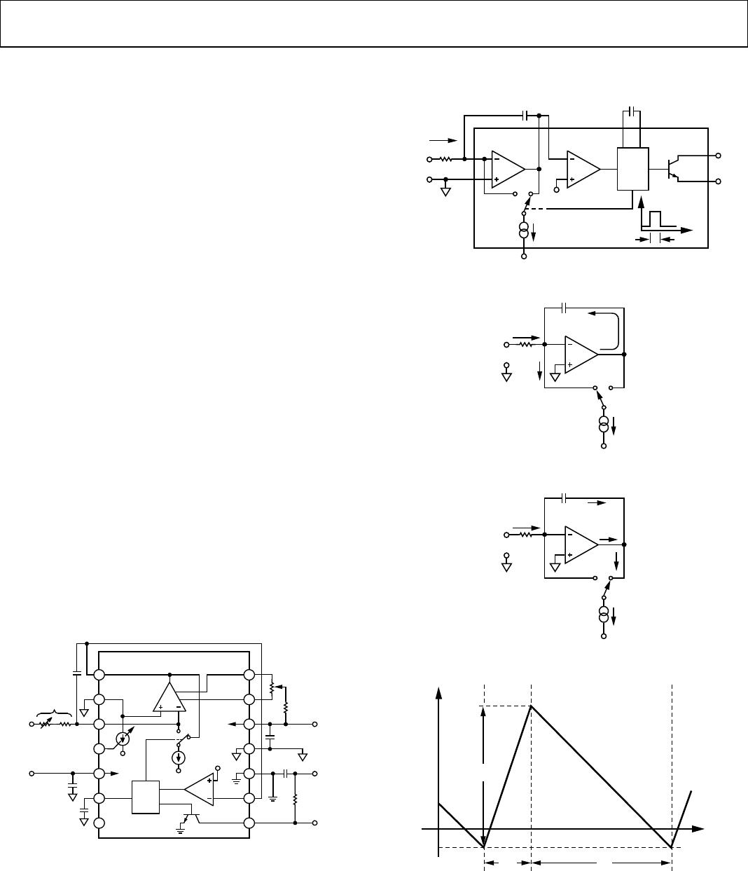
The positive input voltage develops a current (I
IN
= V
IN
/R
IN
) that
charges the integrator capacitor C
INT
. As charge builds up on
C
INT
, the output voltage of the integrator ramps downward
towards ground. When the integrator output voltage (Pin 1)
crosses the comparator threshold (–0.6 V) the comparator
triggers the one shot, whose time period, t
OS
is determined by
the one-shot capacitor C
OS
.
Specifically, the one-shot time period is
sec100.3F/sec108.6
73 −
×+××=
OSOS
Ct
(1)
The reset period is initiated as soon as the integrator output
voltage crosses the comparator threshold, and the integrator
ramps upward by an amount
( )
IN
INT
OS
OS
I
C
t
dt
dV
tV −=×=∆ mA1
(2)
After the reset period has ended, the device starts another
integration period, as shown in Figure 8, and starts ramping
downward again. The amount of time required to reach the
comparator threshold is given as
( )
−=
−
=
∆
= 1
mA1
mA1
1
IN
OS
INT
N
IN
INT
OS
I
t
C
I
I
C
t
dt
dV
V
T
(3)
The output frequency is now given as
FC
RV
A
F
t
I
Tt
f
OS
ININ
OS
IN
OS
OUT
11
1
104.4
/
Hz
15.0
mA1
1
−
×+
×
=
×
=
+
=
(4)
Note that C
INT
, the integration capacitor, has no effect on the
transfer relation, but merely determines the amplitude of the
sawtooth signal out of the integrator.
One-Shot Timing
A key part of the preceding analysis is the one-shot time period
given in Equation 1. This time period can be broken down into
approximately 300 ns of propagation delay and a second time
segment dependent linearly on timing capacitor C
OS
. When the
one shot is triggered, a voltage switch that holds Pin 6 at analog
ground is opened, allowing that voltage to change. An internal
0.5 mA current source connected to Pin 6 then draws its
current out of C
OS
, causing the voltage at Pin 6 to decrease
linearly. At approximately –3.4 V, the one shot resets itself,
thereby ending the timed period and starting the V/F
conversion cycle over again. The total one-shot time period can
be written mathematically as
DELAYGATE
DISCHARGE
OS
OS
T
I
C
V
t +
∆
=
(5)
substituting actual values quoted in Equation 5,
sec10300
A105.0
V4.3
9
3
−
−
×+
×−
×−
=
OS
OS
C
t
(6)
This simplifies into the timed period equation (see Equation 1).
COMPONENT SELECTION
Only four component values must be selected by the user. These
are input resistance R
IN
, timing capacitor C
OS
, logic resistor R2,
and integration capacitor C
INT
. The first two determine the
input voltage and full-scale frequency, while the last two are
determined by other circuit considerations.
Of the four components to be selected, R2 is the easiest to
define. As a pull-up resistor, it should be chosen to limit the
current through the output transistor to 8 mA if a TTL
maximum V
OL
of 0.4 V is desired. For example, if a 5 V logic
supply is used, R2 should be no smaller than 5 V/8 mA or
625 Ω. A larger value can be used if desired.
R
IN
and C
OS
are the only two parameters available to set the full-
scale frequency to accommodate the given signal range. The swing
variable that is affected by the choice of R
IN
and C
OS
is nonlinearity.
The selection guides of Figure 9 and Figure 10 show this quite
graphically. In general, larger values of C
OS
and lower full-scale
input currents (higher values of R
IN
) provide better linearity. In
Figure 10, the implications of four different choices of R
IN
are
shown. Although the selection guide is set up for a unipolar
configuration with a 0 V to 10 V input signal range, the results
can be extended to other configurations and input signal ranges.
For a full-scale frequency of 100 kHz (corresponding to 10 V
input), among the available choices R
IN
= 20 kΩ and C
OS
= 620 pF
gives the lowest nonlinearity, 0.0038%. In addition, the highest
frequency that gives the 20 ppm minimum nonlinearity is
approximately 33 kHz (40.2 kΩ and 1000 pF).
For input signal spans other than 10 V, the input resistance
must be scaled proportionately. For example, if 100 kΩ is called
out for a 0 V to 10 V span, 10 kΩ would be used with a 0 V to 1 V
span, or 200 kΩ with a ±10 V bipolar connection.
The last component to be selected is the integration capacitor
C
INT
. In almost all cases, the best value for C
INT
can be calculated
using the equation
( )
minimumpF1000
sec/10
4
MAX
INT
f
F
C
−
=
(7)
When the proper value for C
INT
is used, the charge balance
architecture of the AD650 provides continuous integration
of the input signal, therefore, large amounts of noise and
interference can be rejected. If the output frequency is
measured by counting pulses during a constant gate period,
the integration provides infinite normal-mode rejection for
frequencies corresponding to the gate period and its harmonics.
However, if the integrator stage becomes saturated by an
excessively large noise pulse, then the continuous integration of
the signal is interrupted, allowing the noise to appear at the output.