RF PLL Frequency Synthesizers
Data Sheet
ADF4110/ADF4111/ADF4112/ADF4113
Rev. F Document Feedback
Information furnished by Analog Devices is believed to be accurate and reliable. However, no
responsibility is assumed by Analog Devices for its use, nor for any infringements of patents or other
rights of third parties that may result from its use. Specifications subject to change without notice. No
license is granted by implication or otherwise under any patent or patent rights of Analog Devices.
Trademarks and registered trademarks are the property of their respective owners.
One Technology Way, P.O. Box 9106, Norwood, MA 02062-9106, U.S.A.
Tel: 781.329.4700 ©2013 Analog Devices, Inc. All rights reserved.
Technical Support www.analog.com
FEATURES
ADF4110: 550 MHz; ADF4111: 1.2 GHz; ADF4112: 3.0 GHz;
ADF4113: 4.0 GHz
2.7 V to 5.5 V power supply
Separate charge pump supply (V
P
) allows extended tuning
voltage in 3 V systems
Programmable dual-modulus prescaler 8/9, 16/17, 32/33,
64/65
Programmable charge pump currents
Programmable antibacklash pulse width
3-wire serial interface
Analog and digital lock detect
Hardware and software power-down mode
APPLICATIONS
Base stations for wireless radio (GSM, PCS, DCS, CDMA,
WCDMA)
Wireless handsets (GSM, PCS, DCS, CDMA, WCDMA)
Wireless LANS
Communications test equipment
CATV equipment
GENERAL DESCRIPTION
The ADF4110 family of frequency synthesizers can be used to
implement local oscillators in the upconversion and downcon-
version sections of wireless receivers and transmitters. They
consist of a low noise digital PFD (phase frequency detector), a
precision charge pump, a programmable reference divider,
programmable A and B counters, and a dual-modulus prescaler
(P/P + 1). The A (6-bit) and B (13-bit) counters, in conjunction
with the dual-modulus prescaler (P/P + 1), implement an N
divider (N = BP + A). In addition, the 14-bit reference counter
(R counter) allows selectable REFIN frequencies at the PFD
input. A complete phase-locked loop (PLL) can be implemented
if the synthesizer is used with an external loop filter and voltage
controlled oscillator (VCO).
Control of all the on-chip registers is via a simple 3-wire
interface. The devices operate with a power supply ranging
from 2.7 V to 5.5 V and can be powered down when not in use.
FUNCTIONAL BLOCK DIAGRAM
N = BP + A
FUNCTION
LATCH
PRESCALER
P/P +1
13-BIT
B COUNTER
6-BIT
A COUNTER
14-BIT
R COUNTER
24-BIT
INPUT REGISTER
R COUNTER
LATCH
A, B COUNTER
LATCH
PHASE
FREQUENCY
DETECTOR
AV
DD
SD
OUT
19
13
14
22
SD
OUT
FROM
FUNCTION
LATCH
DGNDAGNDCE
RF
IN
A
RF
IN
B
LE
DATA
CLK
REF
IN
CPGND
V
P
DV
DD
AV
DD
LOCK
DETECT
ADF4110/ADF4111
ADF4112/ADF4113
6
LOAD
LOAD
REFERENCE
CHARGE
PUMP
M3 M2 M1
HIGH Z
MUX
MUXOUT
CP
R
SET
CURRENT
SETTING 2
CPI3 CPI2 CPI1 CPI6 CPI5 CPI4
CURRENT
SETTING 1
03496-0-001
Figure 1. Functional Block Diagram
ADF4110/ADF4111/ADF4112/ADF4113 Data Sheet
Rev. F | Page 2 of 28
TABLE OF CONTENTS
Features .............................................................................................. 1
Applications ....................................................................................... 1
General Description ......................................................................... 1
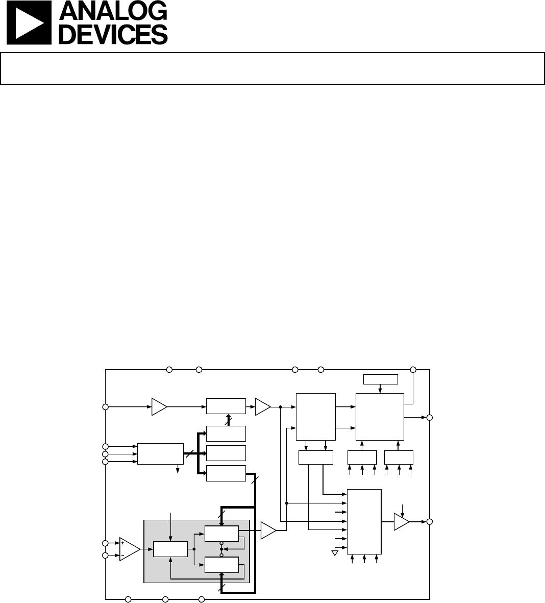
Functional Block Diagram .............................................................. 1
Revision History ............................................................................... 2
Specifications ..................................................................................... 3
Timing Characteristics ..................................................................... 5
Absolute Maximum Ratings ............................................................ 6
Transistor Count ........................................................................... 6
ESD Caution .................................................................................. 6
Pin Configurations and Function Descriptions ........................... 7
Typical Performance Characteristics ............................................. 8
Circuit Description ......................................................................... 12
Reference Input Section ............................................................. 12
RF Input Stage ............................................................................. 12
Prescaler (P/P + 1) ...................................................................... 12
A and B Counters ....................................................................... 12
R Counter .................................................................................... 12
Phase Frequency Detector (PFD) and Charge Pump ............ 13
Muxout and Lock Detect ........................................................... 13
Input Shift Register .................................................................... 13
Function Latch ............................................................................ 19
Initialization Latch ..................................................................... 20
Device Programming after Initial Power-Up ......................... 20
Resynchronizing the Prescaler Output .................................... 21
Applications ..................................................................................... 22
Local Oscillator for GSM Base Station Transmitter .............. 22
Using a D/A Converter to Drive the R
SET
Pin ......................... 23
Shutdown Circuit ....................................................................... 23
Wideband PLL ............................................................................ 23
Direct Conversion Modulator .................................................. 25
Interfacing ................................................................................... 26
PCB Design Guidelines for Chip Scale Package .................... 26
Outline Dimensions ....................................................................... 27
Ordering Guide ............................................................................... 28
REVISION HISTORY
1/13—Rev. E to Rev. F
Changes to Table 1 ............................................................................. 4
Changes to Ordering Guide ........................................................... 28
8/12Rev. D to Rev. E
Changed CP-20-1 to CP-20-6 ........................................... Universal
Updated Outline Dimensions ........................................................ 28
Changes to Ordering Guide ........................................................... 28
5/12Rev. C to Rev. D
Changes to Figure 2 ........................................................................... 5
Changes to Figure 4 and Table 4 ...................................................... 7
Updated Outline Dimensions ........................................................ 28
Changes to Ordering Guide ........................................................... 28
3/04—Data sheet changed from Rev. B to Rev. C.
Updated Format .................................................................. Universal
Changes to Specifications ................................................................. 2
Changes to Figure 32 ....................................................................... 22
Changes to the Ordering Guide ..................................................... 28
3/03Data sheet changed from Rev. A to Rev. B.
Edits to Specifications ....................................................................... 2
Updated OUTLINE DIMENSIONS ............................................. 24
1/01Data sheet changed from Rev. 0 to Rev. A.
Changes to DC Specifications in B Version, B Chips,
Unit, and Test Conditions/Comments Columns ..................... 2
Changes to Absolute Maximum Rating ......................................... 4
Changes to FR
IN
A Function Test ..................................................... 5
Changes to Figure 8 ........................................................................... 7
New Graph AddedTPC 22 ........................................................... 9
Change to PD Polarity Box in Table V ......................................... 15
Change to PD Polarity Box in Table VI ........................................ 16
Change to PD Polarity Paragraph ................................................. 17
Addition of New Material
(PCB Design Guidelines for ChipScale package) ................ 23
Replacement of CP-20 Outline with CP-20 [2] Outline ............ 24
Data Sheet ADF4110/ADF4111/ADF4112/ADF4113
Rev. F | Page 3 of 28
SPECIFICATIONS
AV
DD
= DV
DD
= 3 V ± 10%, 5 V ± 10%; AV
DD
≤V
P
≤ 6.0 V; AGND = DGND = CPGND = 0 V; R
SET
= 4.7 k; dBm referred to 50 Ω;
T
A
= T
MIN
to T
MAX
, unless otherwise noted. Operating temperature range is as follows: B Version: 40°C to +85°C.
Table 1.
Parameter B Version B Chips
1
Unit Test Conditions/Comments
RF CHARACTERISTICS (3 V)
See
Figure 29 for input circuit.
RF Input Sensitivity 15/0 15/0 dBm min/max
RF Input Frequency
ADF4110 80/550 80/550 MHz min/max For lower frequencies, ensure slew rate
(SR) > 30 V/µs.
ADF4110 50/550 50/550 MHz min/max Input level = 10 dBm.
ADF4111 0.08/1.2 0.08/1.2 GHz min/max For lower frequencies, ensure SR > 30 V/µs.
ADF4112 0.2/3.0 0.2/3.0 GHz min/max For lower frequencies, ensure SR > 75 V/µs.
ADF4112 0.1/3.0 0.1/3.0 GHz min/max Input level = 10 dBm.
ADF4113 0.2/3.7 0.2/3.7 GHz min/max Input level = 10 dBm. For lower frequencies,
ensure SR > 130 V/µs.
Maximum Allowable Prescaler Output
Frequency
2
165 165 MHz max
RF CHARACTERISTICS (5 V)
RF Input Sensitivity 10/0 10/0 dBm min/max
RF Input Frequency
ADF4110 80/550 80/550 MHz min/max For lower frequencies, ensure SR > 50 V/µs.
ADF4111
0.08/1.4
0.08/1.4
For lower frequencies, ensure SR > 50 V/µs.
ADF4112 0.1/3.0 0.1/3.0 GHz min/max For lower frequencies, ensure SR > 75 V/µs.
ADF4113 0.2/3.7 0.2/3.7 GHz min/max For lower frequencies, ensure SR > 130 V/µs.
ADF4113 0.2/4.0 0.2/4.0 GHz min/max Input level = 5 dBm.
Maximum Allowable Prescaler Output
Frequency
2
200 200 MHz max
REFIN CHARACTERISTICS
REFIN Input Frequency 5/104 5/104 MHz min/max For f < 5 MHz, ensure SR > 100 V/µs.
Reference Input Sensitivity 0.4/AV
DD
0.4/AV
DD
V p-p min/max AV
DD
= 3.3 V, biased at AV
DD
/2. See Note 3.
3.0/AV
DD
3.0/AV
DD
V p-p min/max
AV
DD
= 5 V, biased at AV
DD
/2. See Note
3
.
REFIN Input Capacitance 10 10 pF max
REFIN Input Current ±100 ±100 µA max
PHASE DETECTOR FREQUENCY
4
55 55 MHz max
CHARGE PUMP
I
CP
Sink/Source
Programmable (see
Table 9).
High Value 5 5 mA typ With R
SET
= 4.7 kΩ.
Low Value 625 625 µA typ
Absolute Accuracy
2.5
2.5
With R
SET
= 4.7 kΩ.
R
SET
Range 2.7/10 2.7/10 kΩ typ
See
Table 9.
I
CP
3-State Leakage Current 1 1 nA typ
Sink and Source Current Matching 2 2 % typ 0.5 V ≤ V
CP
≤ V
P
0.5 V.
I
CP
vs. V
CP
1.5
1.5
0.5 V ≤ V
CP
≤ V
P
0.5 V.
I
CP
vs. Temperature 2 2 % typ V
CP
= V
P
/2.
LOGIC INPUTS
V
INH
, Input High Voltage 0.8 × DV
DD
0.8 × DV
DD
V min
V
INL
, Input Low Voltage
0.2 × DV
DD
0.2 × DV
DD
I
INH
/I
INL
, Input Current ±1 ±1 µA max
C
IN
, Input Capacitance 10 10 pF max
LOGIC OUTPUTS
V
OH
, Output High Voltage DV
DD
0.4 DV
DD
0.4 V min I
OH
= 500 µA.
V
OL
, Output Low Voltage 0.4 0.4 V max I
OL
= 500 µA.

ADF4110BRU-REEL

Mfr. #:
Manufacturer:
Analog Devices Inc.
Description:
Phase Locked Loops - PLL SGL Integer-N 550 MHz
Lifecycle:
New from this manufacturer.
Delivery:
DHL FedEx Ups TNT EMS
Payment:
T/T Paypal Visa MoneyGram Western Union