Data Sheet ADF4110/ADF4111/ADF4112/ADF4113
Rev. F | Page 23 of 28
ADF4111
ADF4112
ADF4113
2.7k
Ω
VCO
GND
18Ω
100pF
100pF
18
Ω
18Ω
RF
OUT
FREF
IN
51
Ω
100pF
100pF
RF
IN
A
RF
IN
B
POWER SUPPLY CONNECTIONS AND DECOUPLING
CAPACITORS ARE OMITTED FOR CLARITY.
R
SET
REF
IN
CP
LOOP
FILTER
CE
CLK
DATA
LE
SPI COMPATIBLE SERIAL BUS
AD5320
12-BIT
V-OUT DAC
MUXOUT
LOCK
DETECT
INPUT
OUTPUT
2
14
6
5
1
8
03496-0-039
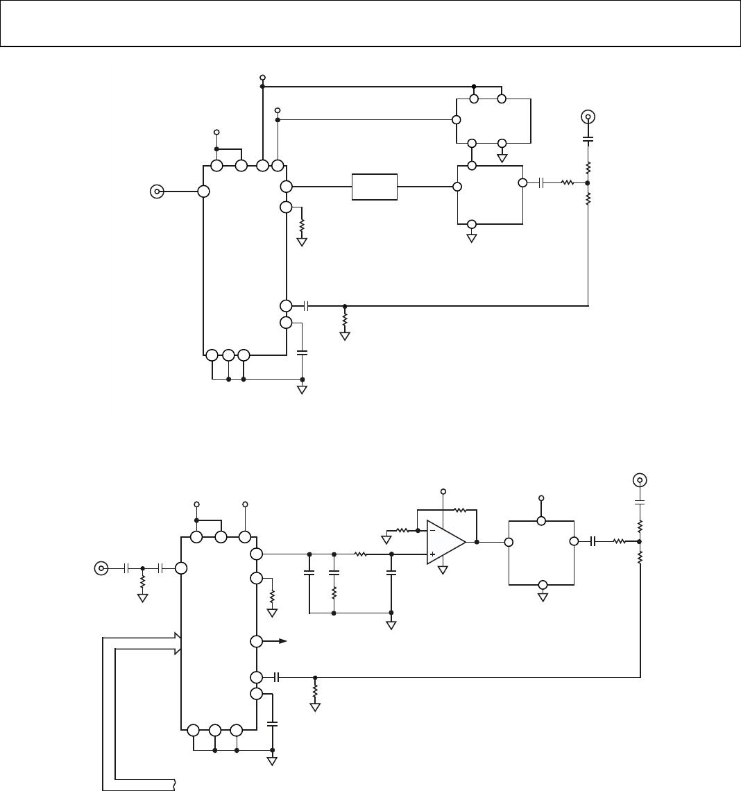
Figure 34. Driving the R
SET
Pin with a D/A Converter
USING A D/A CONVERTER TO DRIVE THE R
SET
PIN
A D/A converter can be used to drive the R
SET
pin of the
ADF4110 family, thus increasing the level of control over the
charge pump current, I
CP
. This can be advantageous in wide-
band applications where the sensitivity of the VCO varies over
the tuning range. To compensate for this, the I
CP
may be varied
to maintain good phase margin and ensure loop stability. See
Figure 34.
SHUTDOWN CIRCUIT
The attached circuit in Figure 35 shows how to shut down both
the ADF4110 family and the accompanying VCO. The ADG701
switch goes closed circuit when a Logic 1 is applied to the IN
input. The low cost switch is available in both SOT-23 and
MSOP packages.
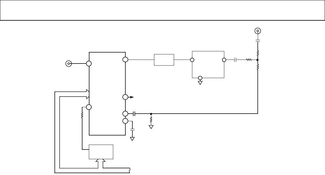
WIDEBAND PLL
Many of the wireless applications for synthesizers and VCOs in
PLLs are narrow band in nature. These applications include the
various wireless standards like GSM, DSC1800, CDMA, and
WCDMA. In each of these cases, the total tuning range for the
local oscillator is less than 100 MHz. However, there are also
wideband applications for which the local oscillator could have
a tuning range as wide as an octave. For example, cable TV
tuners have a total range of about 400 MHz. Figure 36 shows an
application where the ADF4113 is used to control and program
the Micronetics M3500-2235. The loop filter was designed for
an RF output of 2900 MHz, a loop bandwidth of 40 kHz, a PFD
frequency of 1 MHz, I
CP
of 10 mA (2.5 mA synthesizer I
CP
multiplied by the gain factor of 4), VCO K
D
of 90 MHz/V
(sensitivity of the M3500-2235 at an output of 2900 MHz), and
a phase margin of 45°C.
In narrow-band applications, there is generally a small variation
in output frequency (generally less than 10%) and a small
variation in VCO sensitivity over the range (typically 10% to
15%). However, in wideband applications, both of these
parameters have a much greater variation. In Figure 36, for
example, there is a −25% and +17% variation in the RF output
from the nominal 2.9 GHz. The sensitivity of the VCO can vary
from 120 MHz/V at 2750 MHz to 75 MHz/V at 3400 MHz
(+33%, −17%). Variations in these parameters change the loop
bandwidth. This in turn can affect stability and lock time. By
changing the programmable I
CP
, it is possible to get compensa-
tion for these varying loop conditions and ensure that the loop
is always operating close to optimal conditions.