ADF4110/ADF4111/ADF4112/ADF4113 Data Sheet
Rev. F | Page 10 of 28
–140
130
120
–11
0
100
–90
80
–70
–60
50
40
PHASE NOISE (dBc/Hz)
FREQUENCY OFFSET FROM 3100MHz CARRIER (Hz)
10
3
10
2
10
4
10
5
10
6
03496-0-017
RMS NOISE = 1.7°
R
L
= 40dBc/Hz
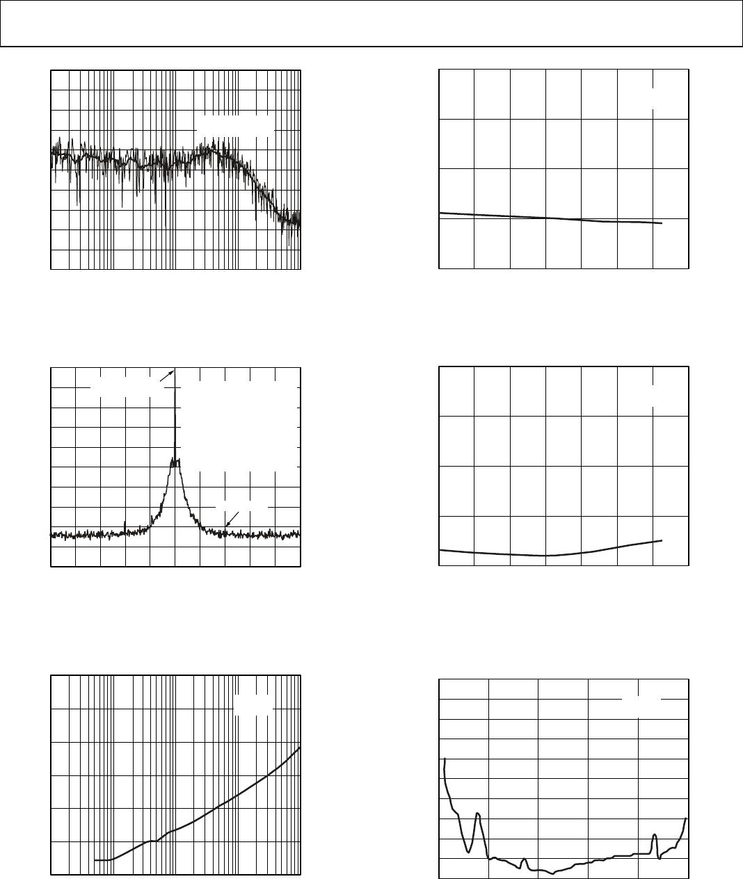
Figure 17. ADF4113 Integrated Phase Noise
(3100 MHz, 1 MHz, 100 kHz)
–100
–90
80
–70
60
50
–40
30
20
10
0
OUTPUT POWER (dB)
–2.0MHz
–1.0MHz
3100MHz
1.0MHz 2.0MHz
FREQUENCY
03496-0-018
V
DD
= 3V, V
P
= 5V
I
CP
= 5mA
PFD FREQUENCY = 1MHz
LOOP BANDWIDTH = 100kHz
RES. BANDWIDTH = 1kHz
VIDEO BANDWIDTH = 1kHz
SWEEP = 13s
AVERAGES = 1
REFERENCE
LEVEL =
17.2dBm
–80.6dBc/Hz
Figure 18. Reference Spurs (3100 MHz, 1 MHz, 100 kHz)
–180
–170
–160
–150
–140
–130
–120
PHASE NOISE (dBc/Hz)
PHASE DETECTOR FREQUENCY (kHz)
101 100 1000 10000
03496-0-019
V
DD
= 3V
V
P
= 5V
Figure 19. ADF4113 Phase Noise (Referred to CP Output)
vs. Phase Detector Frequency
PHASE NOISE (dBc/Hz)
100
–90
–80
–70
–60
–40
–20 0 20 40 60 80 100
TEMPERATURE (°C)
03496-0-020
V
DD
= 3V
V
P
= 3V
Figure 20. ADF4113 Phase Noise vs. Temperature
(900 MHz, 200 kHz, 20 kHz)
FIRST REFERENCE SPUR (dBc)
–100
–90
–80
–70
–60
–40 –20 0 20 40 60 80 100
TEMPERATURE (°C)
03496-0-021
V
DD
= 3V
V
P
= 5V
Figure 21. ADF4113 Reference Spurs vs. Temperature
(900 MHz, 200 kHz, 20 kHz)
–105
–95
–85
–75
–65
–55
–45
–35
–25
–15
–5
FIRST REFERENCE SPUR (dBc)
0 1 2
3 4 5
TUNING VOLTAGE (V)
03496-0-022
V
DD
= 3V
V
P
= 5V
Figure 22. ADF4113 Reference Spurs (200 kHz) vs. V
TUNE
(900 MHz, 200 kHz, 20 kHz)
Data Sheet ADF4110/ADF4111/ADF4112/ADF4113
Rev. F | Page 11 of 28
PHASE NOISE (dBc/Hz)
–100
–90
–80
–70
–60
–40 –20 0 20 40 60 80 100
TEMPERATURE (°C)
03496-0-023
V
DD
= 3V
V
P
= 5V
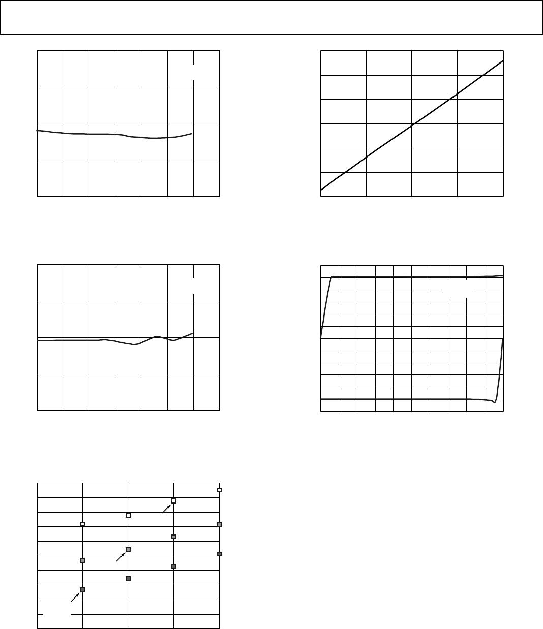
Figure 23. ADF4113 Phase Noise vs. Temperature
(836 MHz, 30 kHz, 3 kHz)
FIRST REFERENCE SPUR (dBc)
100
90
–80
70
60
40 –20
0 20
40
60
80 100
TEMPER
ATURE (
°
C
)
03496-0-024
V
DD
= 3V
V
P
= 5V
Figure 24. ADF4113 Reference Spurs vs. Temperature
(836 MHz, 30 kHz, 3 kHz)
0
1
2
3
4
5
6
7
8
9
10
AI
DD
(mA)
PRESCALER VALUE
8/90 16/17 32/33 64/65
03496-0-025
ADF4113
ADF4112
ADF4110
ADF4111
Figure 25. AI
DD
vs. Prescaler Value
0
0.5
1.0
1.5
2.0
2.5
3.0
DI
DD
(mA)
PRESCALER OUTPUT FREQUENCY (MHz)
500 100 150 200
03496-0-026
V
DD
= 3V
V
P
= 3V
Figure 26. DI
DD
vs. Prescaler Output Frequency
(ADF4110, ADF4111, ADF4112, ADF4113)
–6
4
2
3
–5
0
–1
I
CP
(mA)
2
1
4
3
6
5
0 0.5
1.0
1.5 2.0
2.5
3.0
3.5 4.0 4.5
5.0
V
CP
(V)
03496-0-027
V
PP
= 5V
I
CP
= 5mA
Figure 27. Charge Pump Output Characteristics for ADF4110 Family
ADF4110/ADF4111/ADF4112/ADF4113 Data Sheet
Rev. F | Page 12 of 28
CIRCUIT DESCRIPTION
REFERENCE INPUT SECTION
The reference input stage is shown in Figure 28. SW1 and SW2
are normally closed switches. SW3 is normally open. When
power-down is initiated, SW3 is closed and SW1 and SW2 are
opened. This ensures that there is no loading of the REF
IN
pin
on power-down.
BUFFER
TO R COUNTER
REF
IN
100k
NC
SW2
SW3
NO
NC
SW1
POWER-DOWN
CONTROL
03496-0-028
Figure 28. Reference Input Stage
RF INPUT STAGE
The RF input stage is shown in Figure 29. It is followed by a
two-stage limiting amplifier to generate the current mode logic
(CML) clock levels needed for the prescaler.
AV
DD
AGND
500500
1.6V
BIAS
GENERATOR
RF
IN
A
RF
IN
B
03496-0-029
Figure 29. RF Input Stage
PRESCALER (P/P + 1)
Along with the A and B counters, the dual-modulus prescaler
(P/P + 1) enables the large division ratio, N, to be realized (N =
BP + A). The dual-modulus prescaler, operating at CML levels,
takes the clock from the RF input stage and divides it down to a
manageable frequency for the CMOS A and B counters. The
prescaler is programmable; it can be set in software to 8/9,
16/17, 32/33, or 64/65. It is based on a synchronous 4/5 core.
A AND B COUNTERS
The A and B CMOS counters combine with the dual-modulus
prescaler to allow a wide ranging division ratio in the PLL
feedback counter. The counters are specified to work when the
prescaler output is 200 MHz or less. Thus, with an RF input
frequency of 2.5 GHz, a prescaler value of 16/17 is valid but a
value of 8/9 is not.
Pulse Swallow Function
The A and B counters, in conjunction with the dual-modulus
prescaler, make it possible to generate output frequencies that
are spaced only by the reference frequency divided by
R. The
equation for the VCO frequency is
f
VCO
= [(P × B) + A]f
REFIN
/R
where:
f
VCO
= output frequency of external voltage controlled oscillator
(VCO)
P = preset modulus of dual-modulus prescaler
B = preset divide ratio of binary 13-bit counter(3 to 8191)
A = preset divide ratio of binary 6-bit swallow counter (0 to 63)
f
REFIN
= output frequency of the external reference frequency
oscillator
R = preset divide ratio of binary 14-bit programmable reference
counter (1 to 16383)
R COUNTER
The 14-bit R counter allows the input reference frequency to be
divided down to produce the reference clock to the phase
frequency detector (PFD). Division ratios from 1 to 16,383 are
allowed.
13-BIT B
COUNTER
6-BIT A
COUNTER
PRESCALER
P/P + 1
FROM RF
INPUT STAGE
MODULUS
CONTROL
N = BP + A
LOAD
LOAD
TO PFD
03496-0-030
Figure 30. A and B Counters
ADF4110BRU-REEL

Mfr. #:
Manufacturer:
Analog Devices Inc.
Description:
Phase Locked Loops - PLL SGL Integer-N 550 MHz
Lifecycle:
New from this manufacturer.
Delivery:
DHL FedEx Ups TNT EMS
Payment:
T/T Paypal Visa MoneyGram Western Union