LTC2921/LTC2922 Series
2
29212fa
SYMBOL PARAMETER CONDITIONS MIN TYP MAX UNITS
Supply Pin
V
CC
Supply Voltage Typical Operating Range
LTC2921/LTC2922 4.50 5.00 5.50 V
LTC2921-3.3/LTC2922-3.3 2.97 3.30 3.63 V
LTC2921-2.5/LTC2922-2.5 2.37 2.50 2.63 V
I
CC
Supply Current 2mA
V
CC(MON)
Supply Monitor Threshold Voltage LTC2921/LTC2922 ● 4.285 4.350 4.415 V
LTC2921-3.3/LTC2922-3.3
● 2.828 2.871 2.914 V
LTC2921-2.5/LTC2922-2.5 ● 2.265 2.300 2.335 V
V
CC(OV)
Supply Overvoltage Threshold LTC2921/LTC2922 ● 5.82 6.13 6.43 V
LTC2921-3.3/LTC2922-3.3 ● 3.84 4.04 4.24 V
LTC2921-2.5/LTC2922-2.5
● 3.08 3.24 3.40 V
V
CC
Supply Voltage......................................–0.3V to 7V
V1, V2, V3, V4 Voltages............................... –0.3V to 7V
SENSE Voltage ............................................–0.3V to 7V
TIMER Voltage............................. –0.3V to (V
CC
+ 0.3V)
Charge Pumped Output Voltages
GATE, PG............................................ –0.3V to 12.2V
Switch Voltages
S0, D0, S4, D4 (LTC2922 Series) ............–0.3V to 7V
S1, D1, S2, D2, S3, D3 ............................–0.3V to 7V
ORDER PART
NUMBER
T
JMAX
= 125°C, θ
JA
= 110°C/W
ABSOLUTE AXI U RATI GS
W
WW
U
PACKAGE/ORDER I FOR ATIO
UUW
(Note 1)
ELECTRICAL CHARACTERISTICS
Consult LTC Marketing for parts specified with wider operating temperature ranges.
Switch Currents (DC, RMS)
S0, D0, S4, D4 (LTC2922 Series) ..................... 30mA
S1, D1, S2, D2, S3, D3 ..................................... 30mA
Operating Ambient Temperature Range
LTC2921C/LTC2922C .............................. 0°C to 70°C
LTC2921I/LTC2922I ............................–40°C to 85°C
Junction Temperature (Note 2).............................125°C
Storage Temperature Range ..................–65°C to 150°C
Lead Temperature (Soldering, 10 sec).................. 300°C
ORDER PART
NUMBER
LTC2922CF
LTC2922CF-3.3
LTC2922CF-2.5
LTC2922IF
LTC2922IF-3.3
LTC2922IF-2.5
T
JMAX
= 125°C, θ
JA
= 90°C/W
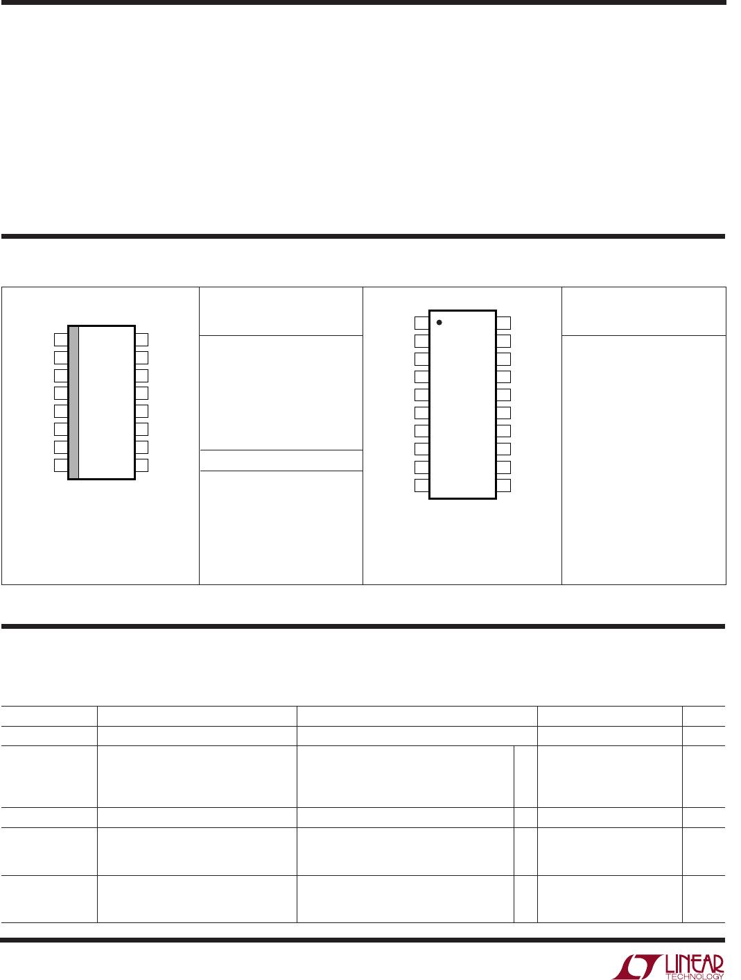
TOP VIEW
GN PACKAGE
16-LEAD NARROW PLASTIC SSOP
1
2
3
4
5
6
7
8
16
15
14
13
12
11
10
9
V1
V2
V3
V4
S3
D3
S2
D2
TIMER
V
CC
SENSE
GATE
PG
GND
D1
S1
1
2
3
4
5
6
7
8
9
10
TOP VIEW
20
19
18
17
16
15
14
13
12
11
SO
TIMER
V1
V2
V3
V4
S4
D4
S3
D3
D0
V
CC
SENSE
GATE
PG
GND
D1
S1
D2
S2
F PACKAGE
20-LEAD PLASTIC TSSOP
LTC2921CGN
LTC2921CGN-3.3
LTC2921CGN-2.5
LTC2921IGN
LTC2921IGN-3.3
LTC2921IGN-2.5
GN PART MARKING
2921
292133
292125
2921I
921I33
921I25
The ● denotes the specifications which apply over the full operating
temperature range, otherwise specifications are at T
A
= 25°C. V
CC
= 5V for LTC2921/LTC2922, V
CC
= 3.3V for
LTC2921-3.3/LTC2922-3.3, and V
CC
= 2.5V for LTC2921-2.5/LTC2922-2.5, unless otherwise noted.

