LTC2921/LTC2922 Series
13
29212fa
APPLICATIO S I FOR ATIO
WUUU
Electronic Circuit Breaker
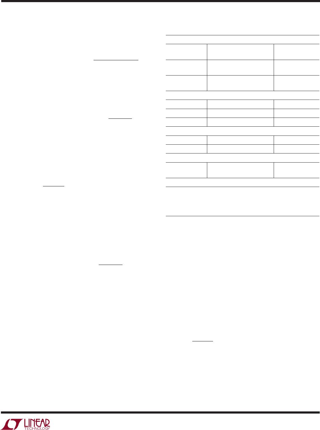
The LTC2921/LTC2922’s electronic circuit breaker pro-
tects against excessive current on V
CC
. The circuit breaker
trips when the SENSE pin falls more than 50mV below the
V
CC
pin for more than 1µs. When the breaker trips, the
remote sense switches are opened and the PG and GATE
pins are pulled to ground, disconnecting the supplies. An
internal latch guarantees that the monitoring sequence
cannot start until the breaker is reset. To reset the circuit
breaker, cycle the V1 input below 0.5V(nom) for more than
150µs. V
CC
falling below the undervoltage threshold also
resets the breaker. After reset, the sequence returns to
Step 1, awaiting valid monitor levels.
Figure 7 shows an equivalent schematic for the electronic
circuit breaker function. Using Equation 8, set the circuit
breaker by selecting R
SENSE
to drop less than the mini-
mum V
SENSE
at the desired trip current:
R
V
I
SENSE
SENSE MIN
LO TRIP
()
()
(8)
After selecting a resistor, use Equations 9a and 9b to
calculate the actual minimum and maximum trip current
threshold limits:
I
V
R
TRIP MIN
SENSE MIN
SENSE MAX
()
()
()
=
(9a)
I
V
R
TRIP MAX
SENSE MAX
SENSE MIN
()
()
()
=
(9b)
Be mindful of thermal effects and power ratings when
choosing a resistor. Place R
SENSE
as close as possible to
the LTC2921/LTC2922 pins to reduce noise pickup, and
use Kelvin sensing to ensure accurate measurement of the
voltage drop. In applications not requiring the current
sensing circuit breaker, tie the SENSE pin to the V
CC
pin.
Configuring the PG Pin Output
The LTC2921 and LTC2922 each include a power good
indicator, the PG pin. During the turn-on sequence, and
upon detection of errors, a strong FET pulls PG to ground
with >10mA of current. When all supplies have satisfied
their monitor and overvoltage thresholds, the circuit breaker
has not tripped, the GATE pin has reached its peak, and the
remote sense switches have turned on, a 4µA current
source from V
PUMP
pulls up PG.
Configure PG as a logic signal by adding an external pull-
up resistor to a voltage source. For example, create a
negative-logic system reset signal by adding an external
pull-up resistor to the load side of a supply voltage, as in
Figure 8. Calculate the minimum pull-up resistor value that
meets the output low voltage specification for V
PG(OL)
:
R
VV
mA
PG MIN
LO MAX
()
()
.
=
04
5
(10)
Do not pull PG above the GATE pin’s fully ramped voltage.
An internal clamp limits the PG voltage to 12.2V relative
to ground. In applications that do not require the PG
output, leave the pin unconnected.
The PG output can also be used as the gate drive for
external N-channel MOSFETs, as in Figure 9. The delay
between the GATE ramp and the PG activation makes a
supply sequencer, useful when two supplies (or two
groups of supplies) need to be ramped one after another.
Choose the FETs and design the ramp rate in the same way
as for the GATE pin. Refer to Equations 5 and 6, substitut-
ing 4µA for 10µA, to choose capacitor C
PG
.
Integrated Switches for Remote Sensing
A significant feature of the LTC2921/LTC2922 series
is a set of remote sense switches that allow for
compensation of voltage drops in the load path. Switch
activation occurs in the turn-on sequence after the GATE
Figure 7. Circuit Breaker Functional Schematic
GATE
ENABLE
CONTROL
LOGIC
V
PUMP
V
PUMP
V
PUMP
SWITCH
ENABLE
PG
ENABLE
4µA
4µA
PG
GATE
REMOTE
SENSE
SWITCH
GATE
LATCH
V
PULSE
WIDTH
MEAS.
+
+
50mV
V
CC
SENSE
R
SENSE
OVERCURRENT
COMPARATOR
V1
V
LO
I
LO
V
SRC0
GND
C
GATE
R
G0
10
2921/22 F07
Q0
LOAD
LTC2922
LTC2921/LTC2922 Series
14
29212fa
APPLICATIO S I FOR ATIO
WUUU
pin has fully ramped up. The switches are N-channel
MOSFETs whose gates are ramped from ground to V
PUMP
at a nominal rate of 8V/ms. The PG pin is activated upon
completion of the TIMER delay cycle that follows GATE
ramp-up and remote sense switch activation. When con-
ditions indicate a supply disconnect, the switches shut off
in less than 10µs.
Figure 10 shows an example of how to connect a switch to
remote sense the load voltage. Although only one remote
sense switch is referred to in this section, the calculations
and comments apply to all.
Before the activation of Q1 and the internal switch, resistor
R
X1
provides a direct path between the DC/DC converter’s
output voltage and its feedback network (R
Y1
and R
Z1
).
Once Q1 activates, the supply energizes the load. When
the internal switch turns on, it provides a remote sense
path between the load voltage and the converter’s feed-
back network.
To choose a value for resistor R
X1
, consider the remote
sense switch connection equivalent network in Figure 11.
Resistor R
Q1(ON)
represents the on-resistance of Q1, and
resistor R
FB1(ON)
represents the on-resistance of the inter-
nal switch.
To allow the load voltage to dominate the feedback to the
converter when the internal switch is closed, make R
X1
>>
R
FB1(ON)
. To set the converter feedback ratio accurately
with R
Y1
and R
Z1
, make both R
X1
and R
FB1(ON)
much less
than (R
Y1
+ R
Z1
). To ensure that most of the load current
flows through the external N-channel FET, choose (R
X1
+
R
FB1(ON)
) >> R
Q1(ON)
. Summarized, these requirements
amount to:
R
Q1(ON)
, R
FB(ON)
<< R
X1
<< (R
Y1
+ R
Z1
) (11)
Approach the selection of R
X1
in the following way: design
the DC/DC converter feedback based on the resistive
divider formed by R
Y1
and R
Z1
with V
S1
at the desired
supply voltage value. When the resistor values satisfy
Equation 11, Equations 12 through 15 are valid.
PG
ENABLE
4µA
PG
V
CC
SENSE
R
SENSE
GATE
V
L0
V
SRC0
GND
C
GATE
R
G0
10
R
PG
2921/22 F08
Q0
LTC2922
µC
RESET
V
PUMP
PG
ENABLE
4µA
PG
V
CC
SENSE
R
SENSE
GATE
V
L0
V
L5
V
SRC0
V
SRC5
GND
C
GATE
C
PG
R
G0
10
R
G5
10
2921/22 F09
Q0
Q5
LTC2922
V
PUMP
2921/22 F10
R
X1
R
Y1
R
Z1
V
SRC1
V
OUT
V
FB
GND
DC/DC
CONVERTER
LTC2922
V1
GND
GATE
Q1
C
GATE
LOAD
R
B1
R
G1
10
R
A1
V
L1
S1
D1
V
S1
2921/22 F11
LTC2922
S1
D1
LOAD
I
DS1
I
Q1
R
X1
R
FB1(ON)
R
Q1(ON)
R
Y1
R
Z1
V
SRC1
V
L1
V
S1
I
L1
V
OUT
V
FB
GND
DC/DC
CONVERTER
Figure 9. PG Pin as Sequenced N-Channel Gate Driver
Figure 8. PG Pin as Logic Output
Figure 10. Automatic Remote Sense Switching Connection
Figure 11. Remote Sense Switch Connection Equivalent Network
LTC2921/LTC2922 Series
15
29212fa
APPLICATIO S I FOR ATIO
WUUU
Before Q1 closes to connect the load, the actual supply
voltage relative to V
S1
is given by Equation 12.
∆= =
++
VVVV
R
RRR
SRC SRC S S
X
XYZ
1111
1
111
–•
(12)
After both Q1 and the internal remote sense switch have
closed, the load voltage relative to V
S1
is given by Equation
13.
∆= =
VVV IR
R
R
LLS LQON
FB ON
X
111 11
1
1
––
()
()
(13)
A small part of the load current will flow through the
remote sense switch. Use Equation 14 to calculate the
current, and do not exceed the switch current Absolute
Maximum Rating when choosing the value of R
X1
.
II
R
R
DS L
QON
X
11
1
1
=
()
(14)
In addition, once the remote sensing is active, the supply
voltage V
SRC1
will rise by approximately the drop across
the external FET. The effect on the monitor resistive divider
design has already been accounted for in the previous
section, Setting the Supply Monitor Levels.
VVIR
R
R
VV
SRC S L Q ON
FB ON
X
SQON
1111
1
1
11
1=+
≈+
••
()
()
()
(15)
The terminals of each switch are interchangeable; choose
the connections to optimize the board layout. Ground all
unused switch pins.
Design Example
Consider the design of a three-supply monitoring system,
as shown in Figure 12, with specifications as listed in
Table␣ 1.
Table 1. Design Example Electrical Specifications
Supply Specifications
5V ± 7.5% V
SRC0(MAX)
= 5.375V I
L0
= 0.8A (max)
V
SRC0(MIN)
= 4.625V
3.3V ± 7.5% V
SRC1(MAX)
= 3.5475V I
L1
= 1.6A (max)
V
SRC1(MIN)
= 3.0525V
2.5V ± 7.5% V
SRC2(MAX)
= 2.6875V I
L2
= 0.4A (max)
V
SRC2(MIN)
= 2.3125V
External N-channel FET Drain-Source Voltage Specification
5V Supply V
Q0(ON)(MAX)
< 250mV
3.3V Supply V
Q1(ON)(MAX)
< 250mV
2.5V Supply V
Q2(ON)(MAX)
< 150mV
Timing Specification
TIMER Delay t
DLY
= 150ms (nom)
GATE Ramp Time t
RAMP
= 500ms (nom)
Bias Current Specification
Monitor Resistive I
A1
= 10µA (nom)
Divider Current I
A2
= 10µA (nom)
Other Requirements
• Remote Sense all 3 Load Voltages
• Tight Monitoring Levels
• Use Circuit Breaker Function
• DC/DC Converter Feedback Resistive Divider >100k
The LTC2921 suits this application because the largest
supply in the system is 5V, and only three remote sense
switches are required.
Start with the design of the resistive dividers that set the
monitor levels. As the largest supply voltage, the 5V
supply must be connected to the V
CC
pin; an internal
resistive divider sets that monitor level. Consult the
Electrical Characteristics table to confirm that V
SRC0(MIN)
>V
CC(MON)(MAX)
and V
SRC0(MAX)
<V
CC(OV)(MIN)
.
The bias current in the lower resistor for the 3.3V supply’s
dividers yields a standard 1% value of R
A1
= 49.9k:
R
V
A
kk
A1
0 500
10
50 49 9=
µ
=≈
.
.

LTC2921CGN-3.3#TRPBF

Mfr. #:
Manufacturer:
Analog Devices Inc.
Description:
Current & Power Monitors & Regulators Power Supply Tracker w/3 FB Switches
Lifecycle:
New from this manufacturer.
Delivery:
DHL FedEx Ups TNT EMS
Payment:
T/T Paypal Visa MoneyGram Western Union