AD7400A Data Sheet
Rev. D | Page 12 of 20
TERMINOLOGY
Differential Nonlinearity
Differential nonlinearity is the difference between the measured
and the ideal 1 LSB change between any two adjacent codes in
the ADC.
Integral Nonlinearity
Integral nonlinearity is the maximum deviation from a straight
line passing through the endpoints of the ADC transfer function.
The endpoints of the transfer function are specified negative
full scale, −250 mV (V
IN
+ − V
IN
−), Code 7169, and specified
positive full scale, +250 mV (V
IN
+ − V
IN
−), Code 58,366 for
the 16-bit level.
Offset Error
Offset is the deviation of the midscale code (Code 32,768 for
the 16-bit level) from the ideal V
IN
+ − V
IN
− (that is, 0 V).
Gain Error
Gain error includes both positive full-scale gain error and
negative full-scale gain error. Positive full-scale gain error is the
deviation of the specified positive full-scale code (58,366 for the
16-bit level) from the ideal V
IN
+ − V
IN
− (+250 mV) after the
offset error is adjusted out. Negative full-scale gain error is the
deviation of the specified negative full-scale code (7169 for the
16-bit level) from the ideal V
IN
+ − V
IN
− (−250 mV) after the
offset error is adjusted out. Gain error includes reference error.
Signal-to-Noise and Distortion (SINAD) Ratio
This ratio is the measured ratio of signal-to-noise and distortion
at the output of the ADC. The signal is the rms amplitude of the
fundamental. Noise is the sum of all nonfundamental signals up
to half the sampling frequency (f
S
/2), excluding dc. The ratio is
dependent on the number of quantization levels in the digitization
process; the more levels, the smaller the quantization noise. The
theoretical signal-to-noise and distortion ratio for an ideal N-bit
converter with a sine wave input is given by
Signal-to-Noise and Distortion = (6.02N + 1.76) dB
Therefore, for a 12-bit converter, SINAD is 74 dB.
Effective Number of Bits (ENOB)
The ENOB is defined by
ENOB = (SINAD − 1.76)/6.02
Total Harmonic Distortion (THD)
THD is the ratio of the rms sum of harmonics to the
fundamental. For the AD7400A, it is defined as
1
6
54
32
V
VVVVV
THD
22222
log20)dB(
++++
=
where:
V
1
is the rms amplitude of the fundamental.
V
2
, V
3
, V
4
, V
5
, and V
6
are the rms amplitudes of the second
through the sixth harmonics.
Peak Harmonic or Spurious Noise
Peak harmonic or spurious noise is defined as the ratio of the rms
value of the next largest component in the ADC output spectrum
(up to f
S
/2, excluding dc) to the rms value of the fundamental.
Normally, the value of this specification is determined by the
largest harmonic in the spectrum, but for ADCs where the
harmonics are buried in the noise floor, it is a noise peak.
Common-Mode Rejection Ratio (CMRR)
CMRR is defined as the ratio of the power in the ADC output at
±250 mV frequency, f, to the power of a 250 mV p-p sine wave
applied to the common-mode voltage of V
IN
+ and V
IN
− of
frequency f
S
as
CMRR (dB) = 10 log(Pf/Pf
S
)
where:
Pf is the power at frequency f in the ADC output.
Pf
S
is the power at frequency f
S
in the ADC output.
Power Supply Rejection Ratio (PSRR)
Variations in power supply affect the full-scale transition but
not the converter linearity. PSRR is the maximum change in the
specified full-scale (±250 mV) transition point due to a change
in power supply voltage from the nominal value (see Figure 6).
Isolation Transient Immunity
The isolation transient immunity specifies the rate of rise/fall of
a transient pulse applied across the isolation boundary beyond
which clock or data is corrupted. (The AD7400A was tested using
a transient pulse frequency of 100 kHz.)
Data Sheet AD7400A
Rev. D | Page 13 of 20
THEORY OF OPERATION
CIRCUIT INFORMATION
The AD7400A isolated Σ-Δ modulator converts an analog input
signal into a high speed (10 MHz typical), single-bit data stream;
the time average of the single-bit data from the modulator is
directly proportional to the input signal. Figure 21 shows a
typical application circuit where the AD7400A is used to provide
isolation between the analog input, a current sensing resistor,
and the digital output, which is then processed by a digital filter
to provide an N-bit word.
ANALOG INPUT
The differential analog input of the AD7400A is implemented
with a switched capacitor circuit. This circuit implements a
second-order modulator stage that digitizes the input signal
into a 1-bit output stream. The sample clock (MCLKOUT)
provides the clock signal for the conversion process as well as
the output data-framing clock. This clock source is internal on
the AD7400A. The analog input signal is continuously sampled
by the modulator and compared to an internal voltage reference. A
digital stream that accurately represents the analog input over
time appears at the output of the converter (see Figure 19).
MODULATOR OUTPUT
+FS ANALOG INPUT
–FS ANALOG INPUT
ANALOG INPUT
07077-019
Figure 19. Analog Input vs. Modulator Output
A differential signal of 0 V ideally results in a stream of 1s and
0s at the MDAT output pin. This output is high 50% of the time
and low 50% of the time. A differential input of 200 mV produces
a stream of 1s and 0s that are high 81.25% of the time (for a
+250 mV input, the output stream is high 89.06% of the time).
A differential input of −200 mV produces a stream of 1s and 0s
that are high 18.75% of the time (for a −250 mV input, the output
stream is high 10.94% of the time).
A differential input of 320 mV ideally results in a stream of all
1s. This is the absolute full-scale range of the AD7400A, while
250 mV is the specified full-scale range, as shown in Table 9.
Table 9. Analog Input Range
Analog Input Voltage Input
Full-Scale Range +640 mV
Positive Full Scale +320 mV
Positive Typical Input Range +250 mV
Positive Specified Input Range +200 mV
Zero 0 mV
Negative Specified Input Range
−200 mV
Negative Typical Input Range −250 mV
Negative Full Scale 320 mV
To reconstruct the original information, this output needs
to be digitally filtered and decimated. A Sinc
3
filter is recom-
mended because this is one order higher than that of the
AD7400A modulator. If a 256 decimation rate is used, the
resulting 16-bit word rate is 39 kHz, assuming a 10 MHz
internal clock frequency. Figure 20 shows the transfer function
of the AD7400A relative to the 16-bit output.
65535
53248
SPECIFIED RANGE
ANALOG INPUT
ADC CODE
12288
–320mV –200mV +200mV
+320mV
0
07077-020
Figure 20. Filtered and Decimated 16-Bit Transfer Characteristic
Σ-Δ
MOD/
ENCODER
INPUT
CURRENT
NONISOLATED
5V/3V
ISOLATED
5V
V
DD1
R
SHUNT
V
IN
+
V
IN
GND
1
V
DD
GND
V
DD2
MDAT MDAT
SINC
3
FILTER*
AD7400A
MCLKOUT
SDAT
CS
SCLK
MCLK
GND
2
DECODER
DECODER
+
ENCODER
07077-018
*THIS FILTER IS IMPLEMENTED
WITH AN FPGA OR DSP.
Figure 21. Typical Application Circuit
AD7400A Data Sheet
Rev. D | Page 14 of 20
DIFFERENTIAL INPUTS
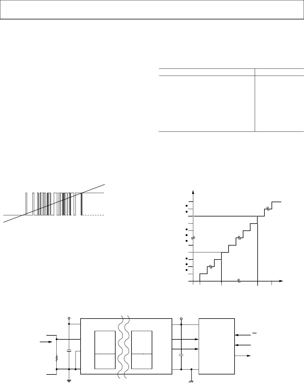
The analog input to the modulator is a switched capacitor
design. The analog signal is converted into charge by highly
linear sampling capacitors. A simplified equivalent circuit
diagram of the analog input is shown in Figure 22. A signal
source driving the analog input must be able to provide the
charge onto the sampling capacitors every half MCLKOUT cycle
and settle to the required accuracy within the next half cycle.
φA
φB
1kΩ
V
IN
φA
φB
φB φB
1kΩ
V
IN
+
2pF
2pF
φA φA
MCLKOUT
07077-027
Figure 22. Analog Input Equivalent Circuit
Because the AD7400A samples the differential voltage across its
analog inputs, low noise performance is attained with an input
circuit that provides low common-mode noise at each input.
The amplifiers used to drive the analog inputs play a critical
role in attaining the high performance available from the
AD7400A.
When a capacitive load is switched onto the output of an op
amp, the amplitude drops momentarily. The op amp tries to
correct the situation and, in the process, hits its slew rate limit.
This nonlinear response, which can cause excessive ringing, can
lead to distortion. To remedy the situation, a low-pass RC filter
can be connected between the amplifier and the input to the
AD7400A. The external capacitor at each input aids in supplying
the current spikes created during the sampling process, and the
resistor isolates the op amp from the transient nature of the load.
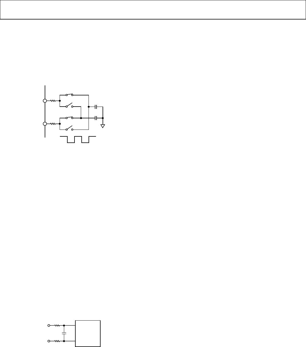
The recommended circuit configuration for driving the differential
inputs to achieve best performance is shown in Figure 23. A
capacitor between the two input pins sources or sinks charge
to allow most of the charge that is needed by one input to be
effectively supplied by the other input. The series resistor again
isolates any op amp from the current spikes created during the
sampling process. Recommended values for the resistors and
capacitor are 22 Ω and 47 pF, respectively.
R
V
IN
R
V
IN
+
C
AD7400A
07077-028
Figure 23. Differential Input RC Network
CURRENT SENSING APPLICATIONS
The AD7400A is ideally suited for current sensing applications
where the voltage across a shunt resistor is monitored. The load
current flowing through an external shunt resistor produces a
voltage at the input terminals of the AD7400A. The AD7400A
provides isolation between the analog input from the current
sensing resistor and the digital outputs. By selecting the appropriate
shunt resistor value, a variety of current ranges can be monitored.
Choosing R
SENSE
The shunt resistor values used in conjunction with the AD7400A
are determined by the specific application requirements in terms of
voltage, current, and power. Small resistors minimize power
dissipation, while low inductance resistors prevent any induced
voltage spikes, and good tolerance devices reduce current
variations. The final values chosen are a compromise between
low power dissipation and good accuracy. Low value resistors
have less power dissipated in them, but higher value resistors
may be required to use the full input range of the ADC, thus
achieving maximum SNR performance.
When the peak sense current is known, the voltage range of the
AD7400A (±200 mV) is divided by the maximum sense current
to yield a suitable shunt value. If the power dissipation in the shunt
resistor is too large, the shunt resistor can be reduced, in which
case, less of the ADC input range is used. Using less of the ADC
input range results in performance that is more susceptible to noise
and offset errors because offset errors are fixed and are thus more
significant when smaller input ranges are used.
R
SENSE
must be able to dissipate the I2R power losses. If the power
dissipation rating of the resistor is exceeded, its value may drift
or the resistor may be damaged, resulting in an open circuit.
This can result in a differential voltage across the terminals of
the AD400A in excess of the absolute maximum ratings (see
Table 6.). If I
SENSE
has a large high frequency component, take
care to choose a resistor with low inductance.
VOLTAGE SENSING APPLICATIONS
The AD7400A can also be used for isolated voltage monitoring.
For example, in motor control applications, it can be used to
sense bus voltage. In applications where the voltage being
monitored exceeds the specified analog input range of the
AD7400A, a voltage divider network can be used to reduce
the voltage being monitored to the required range.

AD7400AYNSZ

Mfr. #:
Manufacturer:
Analog Devices Inc.
Description:
IC MODULATOR SIGMADELTA 8-SMD
Lifecycle:
New from this manufacturer.
Delivery:
DHL FedEx Ups TNT EMS
Payment:
T/T Paypal Visa MoneyGram Western Union

Products related to this Datasheet