AD7400A Data Sheet
Rev. D | Page 6 of 20
DIN V VDE V 0884-10 (VDE V 0884-10) INSULATION CHARACTERISTICS
This isolator is suitable for reinforced electrical isolation only within the safety limit data. Maintenance of the safety data is ensured by
means of protective circuits.
Table 5.
Parameter Symbol Characteristic Unit
INSTALLATION CLASSIFICATION PER DIN VDE 0110
For Rated Mains Voltage 300 V rms I to IV
For Rated Mains Voltage 450 V rms I to II
For Rated Mains Voltage 600 V rms I to II
CLIMATIC CLASSIFICATION 40/105/21
POLLUTION DEGREE (DIN VDE 0110, Table 1) 2
MAXIMUM WORKING INSULATION VOLTAGE V
IORM
891 V peak
INPUT-TO-OUTPUT TEST VOLTAGE, METHOD B1
V
IORM
× 1.875 = V
PR
, 100% Production Test, t
m
= 1 sec, Partial Discharge < 5 pC V
PR
1671 V peak
INPUT-TO-OUTPUT TEST VOLTAGE, METHOD A V
PR
After Environmental Test Subgroup 1 1426 V peak
V
IORM
× 1.6 = V
PR
, t
m
= 60 sec, Partial Discharge < 5 pC
After Input and/or Safety Test Subgroup 2/Safety Test Subgroup 3 1069 V peak
V
IORM
× 1.2 = V
PR
, t
m
= 60 sec, Partial Discharge < 5 pC
HIGHEST ALLOWABLE OVERVOLTAGE (TRANSIENT OVERVOLTAGE, t
TR
= 10 sec) V
TR
6000 V peak
SAFETY-LIMITING VALUES (MAXIMUM VALUE ALLOWED IN THE EVENT OF A FAILURE, ALSO SEE Figure 4)
Case Temperature T
S
150 °C
Side 1 Current
I
S1
265
mA
Side 2 Current
I
S2
335
mA
INSULATION RESISTANCE AT T
S
, V
IO
= 500 V R
S
>10
9
CASE TEMPERATURE (°C)
SAFETY-LIMITING CURRENT (mA)
0
0
350
300
250
200
150
100
50
50 100
150 200
SIDE 1
SIDE 2
07077-026
Figure 4. Thermal Derating Curve, Dependence of Safety-Limiting Values
with Case Temperature per DIN V VDE V 0884-10
Data Sheet AD7400A
Rev. D | Page 7 of 20
ABSOLUTE MAXIMUM RATINGS
T
A
= 25°C, unless otherwise noted. All voltages are relative to
their respective ground.
Table 6.
Parameter Rating
V
DD1
to GND
1
−0.3 V to +6.5 V
V
DD2
to GND
2
−0.3 V to +6.5 V
Analog Input Voltage to GND
1
−0.3 V to V
DD1
+ 0.3 V
Output Voltage to GND
2
−0.3 V to V
DD2
+ 0.3 V
Input Current to Any Pin Except Supplies
1
±10 mA
Operating Temperature Range −40°C to +125°C
Storage Temperature Range −65°C to +150°C
Junction Temperature 150°C
SOIC Package
θ
JA
Thermal Impedance
2
89.2°C/W
θ
JC
Thermal Impedance
2
55.6°C/W
Resistance (Input-to-Output), R
I-O
10
12
Capacitance (Input-to-Output), C
I-O
3
1.7 pF typ
RoHS-Compliant Temperature, Soldering
Reflow 260 (+0)°C
ESD
2.5 kV
1
Transient currents of up to 100 mA do not cause SCR to latch-up.
2
JEDEC 2S2P standard board.
3
f = 1 MHz.
Stresses above those listed under Absolute Maximum Ratings
may cause permanent damage to the device. This is a stress
rating only; functional operation of the device at these or any
other conditions above those indicated in the operational
section of this specification is not implied. Exposure to absolute
maximum rating conditions for extended periods may affect
device reliability.
Table 7. Maximum Continuous Working Voltage
1
Parameter Max Unit Constraint
AC Voltage,
Bipolar Waveform
565 V peak 50-year minimum
lifetime
AC Voltage,
Unipolar Waveform
891 V peak Maximum CSA/VDE
approved working
voltage
DC Voltage 891 V Maximum CSA/VDE
approved working
voltage
1
Refers to continuous voltage magnitude imposed across the isolation
barrier. See the Insulation Lifetime section for more details.
ESD CAUTION
AD7400A Data Sheet
Rev. D | Page 8 of 20
PIN CONFIGURATION AND FUNCTION DESCRIPTIONS
07077-104
NC = NO CONNECT
AD7400A
TOP VIEW
(Not to Scale)
V
DD1
V
DD2
V
IN
+
V
IN
GND
2
GND
2
V
DD1
/NC
GND
1
1
2
3
NC
4
NC
5
NC
MCLKOUT
NC
16
15
14
NC
6
7
8
MDAT
NC
11
10
9
13
12
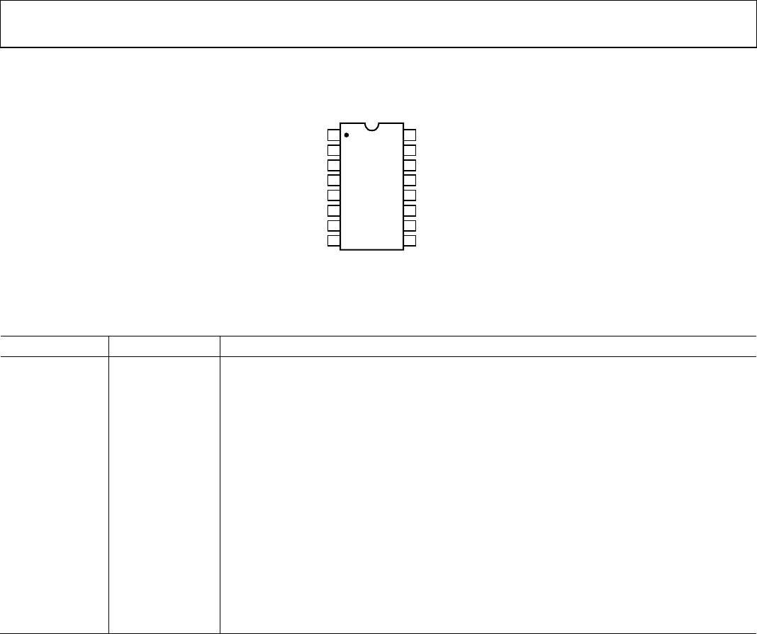
Figure 5. Pin Configuration
Table 8. Pin Function Descriptions
Pin No. Mnemonic Description
1 V
DD1
Supply Voltage, 4.5 V to 5.5 V. This is the supply voltage for the isolated side of the AD7400A and is
relative to GND
1
.
2 V
IN
+ Positive Analog Input. Specified range of ±250 mV.
3 V
IN
Negative Analog Input. Normally connected to GND
1
.
4 to 6, 10, 12, 15 NC No Connect.
7 V
DD1
/NC
Supply Voltage. 4.5 V to 5.5 V. This is the supply voltage for the isolated side of the AD7400A and is
relative to GND
1
.
No Connect (NC). If desired, Pin 7 of the SOIC device may be allowed to float. It should not be tied
to ground. The AD7400A will operate normally provided that the supply voltage is applied to Pin 1.
8 GND
1
Ground 1. This is the ground reference point for all circuitry on the isolated side.
9, 16 GND
2
Ground 2. This is the ground reference point for all circuitry on the nonisolated side.
11 MDAT
Serial Data Output. The single bit modulator output is supplied to this pin as a serial data stream. The
bits are clocked out on the rising edge of the MCLKOUT output and are valid on the following
MCLKOUT rising edge.
13 MCLKOUT
Master Clock Logic Output (10 MHz Typical). The bit stream from the modulator is valid on the
rising edge of MCLKOUT.
14 V
DD2
Supply Voltage, 3 V to 5.5 V. This is the supply voltage for the nonisolated side and is relative to GND
2
.

AD7400AYNSZ

Mfr. #:
Manufacturer:
Analog Devices Inc.
Description:
IC MODULATOR SIGMADELTA 8-SMD
Lifecycle:
New from this manufacturer.
Delivery:
DHL FedEx Ups TNT EMS
Payment:
T/T Paypal Visa MoneyGram Western Union

Products related to this Datasheet