Data Sheet AD7400A
Rev. D | Page 15 of 20
DIGITAL FILTER
The overall system resolution and throughput rate is deter-
mined by the filter selected and the decimation rate used. The
higher the decimation rate, the greater the system accuracy, as
illustrated in Figure 24. However, there is a tradeoff between
accuracy and throughput rate and, therefore, higher decimal-
tion rates result in lower throughput solutions.
A Sinc
3
filter is recommended for use with the AD7400A. This
filter can be implemented on an FPGA or a D S P.
( )
( )
3
1
1
1
)(
=
Z
Z
zH
DR
where DR is the decimation rate.
80
70
60
50
40
30
20
10
0
90
10 100 1k1
DECIMATION RATE
SNR (dB)
SINC
3
SINC
2
SINC
1
07077-025
Figure 24. SNR vs. Decimation Rate for Different Filter Types
The following Verilog code provides an example of a Sinc
3
filter
implementation on a Xilinx® Spartan-II 2.5 V FPGA. This code
can possibly be compiled for another FPGA, such as an Altera®
device. Note that the data is read on the negative clock edge in
this case, although it can be read on the positive edge, if preferred.
Figure 24 shows the effect of using different decimation rates
with various filter types.
/*`Data is read on negative clk edge*/
module DEC256SINC24B(mdata1, mclk1, reset,
DATA);
input mclk1; /*used to clk filter*/
input reset; /*used to reset filter*/
input mdata1; /*ip data to be
filtered*/
output [15:0] DATA; /*filtered op*/
integer location;
integer info_file;
reg [23:0] ip_data1;
reg [23:0] acc1;
reg [23:0] acc2;
reg [23:0] acc3;
reg [23:0] acc3_d1;
reg [23:0] acc3_d2;
reg [23:0] diff1;
reg [23:0] diff2;
reg [23:0] diff3;
reg [23:0] diff1_d;
reg [23:0] diff2_d;
reg [15:0] DATA;
reg [7:0] word_count;
reg word_clk;
reg init;
/*Perform the Sinc ACTION*/
always @ (mdata1)
if(mdata1==0)
ip_data1 <= 0; /* change from a 0
to a -1 for 2's comp */
else
ip_data1 <= 1;
/*ACCUMULATOR (INTEGRATOR)
Perform the accumulation (IIR) at the speed
of the modulator.
MCLKOUT
IP_DATA1
ACC1+
ACC2+
ACC3+
+
Z
+
Z
+
Z
07077-021
Figure 25. Accumulator
Z = one sample delay
MCLKOUT = modulators conversion bit rate
*/
always @ (negedge mclk1 or posedge reset)
if (reset)
begin
/*initialize acc registers on reset*/
acc1 <= 0;
acc2 <= 0;
acc3 <= 0;
end
else
begin
/*perform accumulation process*/
acc1 <= acc1 + ip_data1;
acc2 <= acc2 + acc1;
acc3 <= acc3 + acc2;
end
/*DECIMATION STAGE (MCLKOUT/ WORD_CLK)
*/
always @ (posedge mclk1 or posedge reset)
if (reset)
word_count <= 0;
else
word_count <= word_count + 1;
always @ (word_count)
word_clk <= word_count[7];
AD7400A Data Sheet
Rev. D | Page 16 of 20
/*DIFFERENTIATOR (including decimation
stage)
Perform the differentiation stage (FIR) at a
lower speed.
+
+
Z
–1
+
Z
–1
Z
–1
ACC3
DIFF1
DIFF2 DIFF3
WORD_CLK
07077-022
Figure 26. Differentiator
Z = one sample delay
WORD_CLK = output word rate
*/
always @ (posedge word_clk or posedge reset)
if(reset)
begin
acc3_d2 <= 0;
diff1_d <= 0;
diff2_d <= 0;
diff1 <= 0;
diff2 <= 0;
diff3 <= 0;
end
else
begin
diff1 <= acc3 - acc3_d2;
diff2 <= diff1 - diff1_d;
diff3 <= diff2 - diff2_d;
acc3_d2 <= acc3;
diff1_d <= diff1;
diff2_d <= diff2;
end
/* Clock the Sinc output into an output
register
WORD_CLK
DATADIFF3
07077-023
Figure 27. Clocking Sinc Output into an Output Register
WORD_CLK = output word rate
*/
always @ (posedge word_clk)
begin
DATA[15] <= diff3[23];
DATA[14] <= diff3[22];
DATA[13] <= diff3[21];
DATA[12] <= diff3[20];
DATA[11] <= diff3[19];
DATA[10] <= diff3[18];
DATA[9] <= diff3[17];
DATA[8] <= diff3[16];
DATA[7] <= diff3[15];
DATA[6] <= diff3[14];
DATA[5] <= diff3[13];
DATA[4] <= diff3[12];
DATA[3] <= diff3[11];
DATA[2] <= diff3[10];
DATA[1] <= diff3[9];
DATA[0] <= diff3[8];
end
endmodule
Data Sheet AD7400A
Rev. D | Page 17 of 20
APPLICATIONS INFORMATION
GROUNDING AND LAYOUT
Supply decoupling with a value of 100 nF is strongly recom-
mended on both V
DD1
and V
DD2
. Decoupling on one or
both V
DDx
pins does not significantly affect performance. In
applications involving high common-mode transients, ensure
that board coupling across the isolation barrier is minimized.
Furthermore, the board layout should be designed so that
any coupling that occurs equally affects all pins on a given
component side. Failure to ensure this may cause voltage
differentials between pins to exceed the absolute maximum
ratings of the device, thereby leading to latch-up or permanent
damage. Any decoupling used should be placed as close to the
supply pins as possible.
Series resistance in the analog inputs should be minimized to
avoid any distortion effects, especially at high temperatures. If
possible, equalize the source impedance on each analog input to
minimize offset. Beware of mismatch and thermocouple effects
on the analog input PCB tracks to reduce offset drift.
EVALUATING THE AD7400A PERFORMANCE
An AD7400A evaluation board is available with split ground
planes and a board split beneath the AD7400A package to
ensure isolation. This board allows access to each pin on the
device for evaluation purposes.
The evaluation board package includes a fully assembled and
tested evaluation board, documentation, and software for
controlling the board from the PC via the EVA L -CED1Z. The
software also includes a SINC
3
filter implemented on an FPGA.
The evaluation board is used in conjunction with the EVAL-CED1Z
board and can be used as a standalone board. The software
allows the user to perform ac (fast Fourier transform) and dc
(histogram of codes) tests on the AD7400A. The software and
documentation are on a CD that ships with the evaluation board.
INSULATION LIFETIME
All insulation structures subjected to sufficient time and/or
voltage are vulnerable to breakdown. In addition to the testing
performed by the regulatory agencies, Analog Devices has carried
out an extensive set of evaluations to determine the lifetime of
the insulation structure within the AD7400A.
These tests subjected populations of devices to continuous
cross-isolation voltages. To accelerate the occurrence of failures,
the selected test voltages were values exceeding those of normal
use. The time to failure values of these units were recorded and
used to calculate acceleration factors. These factors were then
used to calculate the time to failure under normal operating
conditions. The values shown in Table 7 are the lesser of the
following two values:
The value that ensures at least a 50-year lifetime of
continuous use.
The maximum CSA/VDE approved working voltage.
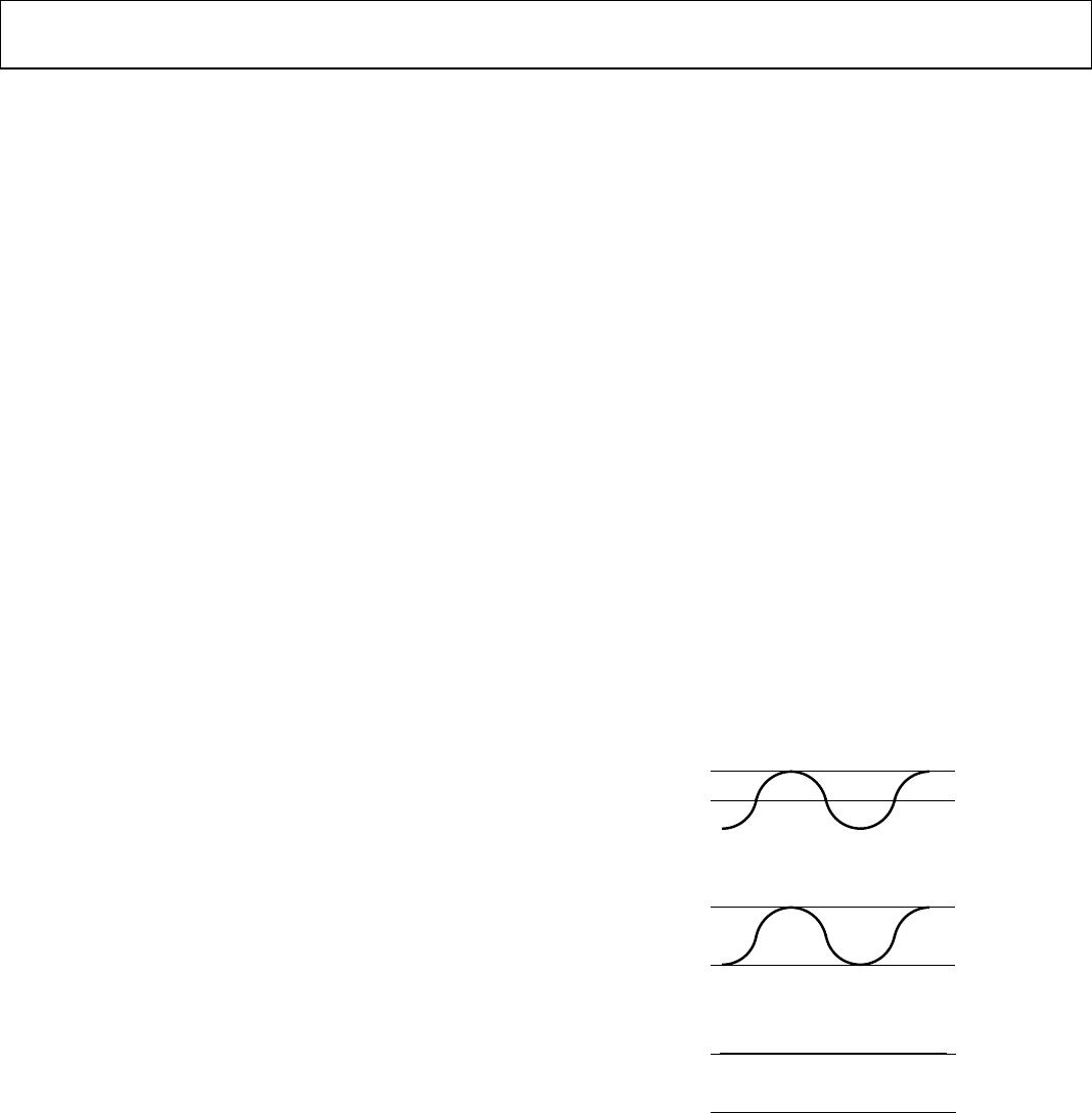
Note that the lifetime of the AD7400A varies according to
the waveform type imposed across the isolation barrier. The
iCoupler insulation structure is stressed differently depending
on whether the waveform is bipolar ac, unipolar ac, or dc.
Figure 28, Figure 29, and Figure 30 illustrate the different
isolation voltage waveforms.
0V
RATED PEAK VOLTAGE
07077-029
Figure 28. Bipolar AC Waveform
0V
RATED PEAK VOLTAGE
07077-030
Figure 29. Unipolar AC Waveform
0V
RATED PEAK VOLTAGE
07077-031
Figure 30. DC Waveform

AD7400AYNSZ

Mfr. #:
Manufacturer:
Analog Devices Inc.
Description:
IC MODULATOR SIGMADELTA 8-SMD
Lifecycle:
New from this manufacturer.
Delivery:
DHL FedEx Ups TNT EMS
Payment:
T/T Paypal Visa MoneyGram Western Union

Products related to this Datasheet