34 DS580F6
CS8406
14.ORDERING INFORMATION
Product Description Pb-Free Package Grade Temp Range Container Order#
CS8406
192 kHz Digital Audio
Transmitter
YES
SOIC
Commer-
cial
-10º to +70ºC
Rail CS8406-CSZ
Tape and Reel CS8406-CSZR
Automotive -40º to +85ºC
Rail CS8406-DSZ
Tape and Reel CS8406-DSZR
TSSOP
Commer-
cial
-10º to +70ºC
Rail CS8406-CZZ
Tape and Reel CS8406-CZZR
Automotive -40º to +85ºC
Rail CS8406-DZZ
Tape and Reel CS8406-DZZR
CDB8416
CS8406 & CS8416 Evaluation
Board
- - - - CDB8416
DS580F6 35
CS8406
15.APPENDIX A: EXTERNAL AES3/SPDIF/IEC60958 TRANSMITTER
COMPONENTS
This section details the external components required to interface the AES3 transmitter to cables and fiber-optic
components.
15.1 AES3 Transmitter External Components
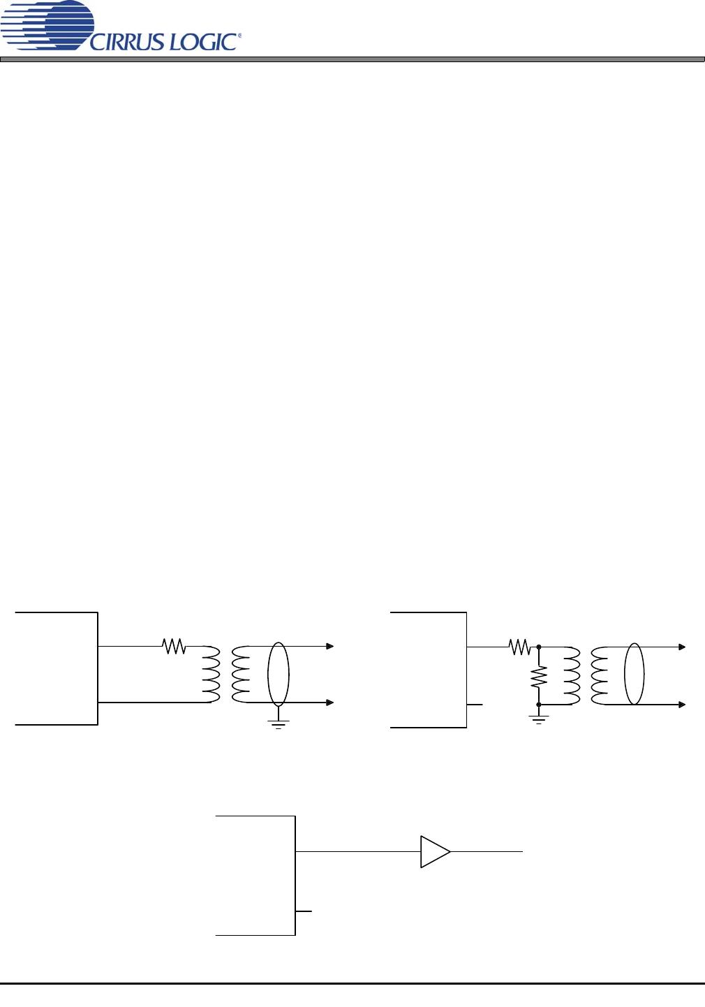
The output drivers on the CS8406 are designed to drive both the professional and consumer interfaces. The
AES3 and IEC60958-4 specifications call for a balanced output drive of 2-7 V peak-to-peak into a 110
±
20% load with no cable attached. Using the circuit in Figure 14, the output of the transformer is short-circuit
protected, has the p roper source impedance, and provides a 5 V peak-to-peak signal into a 110
load.
Lastly, the two output pins should be attached to an XLR connector with male pins and a female shell, and
with pin 1 of the connector grounded.
In the case of consumer use, the IEC60958-3 specification calls for an unbalanced drive circuit with an out-
put impedance of 75
± 20% and a output drive level of 0.5 V peak-to-peak ± 20% when measured across
a 75
load using no cable. The circuit shown in Figure 15 only uses the TXP pin and provides the proper
output impedance and drive level using standard 1% resistors. If VL is set to +3.3 V, change 374
to 243
and change 90.9 to 107 . The connector for a consumer application would be an RCA phono socket.
This circuit is also short circuit protected.
The TXP pin may be used to drive TTL or CMOS gates as shown in Figure 16. This circuit may be used for
optical connectors for digital audio since they usually have TTL or CMOS compatible inputs. This circuit is
also useful when driving multiple digital audio outputs since RS422 line drivers have TTL compatible inputs.
15.2 Isolating Transformer Requirements
Please refer to the application note AN134: AES and SPDIF Recommended Transformers for resources on
transformer selection.
374-R
TXP
90.9
TXP
TXN
RCA
Phono
CS8406
110-(R
TXP
+R
TXN
)
TXP
TXN
XLR
Pin 1
CS8406
Figure 14. Professional Output Circuit Figure 15. Consumer Output Circuit (VL = 5.0 V)
TXP
TXN
TTL or
CMOS Gate
CS8406
Figure 16. TTL/CMOS Output Circuit
36 DS580F6
CS8406
16.APPENDIX B: CHANNEL STATUS AND USER DATA BUFFER
MANAGEMENT
The CS8406 has a comprehensive channel status (C) and user (U) data buffering scheme which allows the user to
manage the C and U data through the control port.
16.1 AES3 Channel Status(C) Bit Management
The CS8406 contains sufficient RAM to store a full block of C data for both A and B channels (192x2 = 384
bits), and also 384 bits of U information. The user may read from or write to these RAM buffers through the
control port.
The CS8406 manages the flow of channel status data at the block level, meaning that entire blocks of chan-
nel status information are buffered at the input, synchronized to the output timebase, and then transmitted.
The buffering scheme involves a cascade of 2 block-sized buffers, named E and F, as shown in Figure 17.
The MSB of each byte represents the first bit in the serial C data stream. For example, the MSB of byte 0
(which is at control port address 20h) is the consumer/professional bit for channel status block A.
The E buffer is accessible from the control port, allowing read and writing of the C data. The F buffer is used
as the source of C data for the AES3 transmitter. The F buffer accepts block transfers from the E buffer.
16.1.1 Accessing the E buffer
The user can monitor the data being transferred by reading the E buffer, which is mapped into the register
space of the CS8406, through the control port. The user can modify the data to be transmitted by writing
to the E buffer.
The user can configure the interrupt enable register to cause interrupts to occur whenever “E to F” buffer
transfers occur. This allows determination of the allowable time periods to interact with the E buffer.
Also provided is an “E to F” inhibit bit. The “E to F” buffer transfer is disabled whenever the user sets this
bit. This may be used whenever “long” control port interactions are occurring.
A flowchart for reading and writing to the E buffer is shown in Figure 18. For writing, the sequence starts
after a E to F transfer, which is based on the output timebase.
If the channel status block to transmit indicates PRO Mode, then the CRCC byte is automatically calcu-
lated by the CS8406, and does not have to be written into the last byte of the block by the host microcon-
Control Port
To
AES3
Transmitter
E
24
words
8-bits 8-bits
AB
F
Transmit
Data
Buffer
Figure 17. Channel Status Data Buffer Structure

CS8406-DSZ

Mfr. #:
Manufacturer:
Cirrus Logic
Description:
Audio Transmitters, Receivers, Transceivers 192kHz Digital Audio Transmitter
Lifecycle:
New from this manufacturer.
Delivery:
DHL FedEx Ups TNT EMS
Payment:
T/T Paypal Visa MoneyGram Western Union