DS580F6 37
CS8406
troller. This is also true if the channel status data is entered serially through the COPY/C pin when the part
is in Hardware Mode.
16.1.2 Serial Copy Management System (SCMS)
In Software Mode, the CS8406 allows read/modify/write access to all the channel status bits. For Con-
sumer Mode SCMS compliance, the host microcontroller needs to manipulate the Category Code, Copy
bit and L bit appropriately.
In Hardware Mode, the SCMS protocol can be followed by either using the COPY and ORIG input pins,
or by using the C bit serial input pin. These options are documented in the Hardware Mode section of this
data sheet.
16.1.3 Channel Status Data E Buffer Access
The E buffer is organized as 24 x 16-bit words. For each word the MS Byte is the A channel data, and the
LS Byte is the B channel data (see Figure 17).
There are two methods of accessing this memory, known as One-Byte Mode and Two-Byte Mode. The
desired mode is selected through a control register bit.
16.1.3.1 One-Byte Mode
In many applications, the channel status blocks for the A and B channels will be identical. In this situation,
if the user reads a byte from one of the channel's blocks, the corresponding byte for the other channel will
be the same. Similarly, if the user wrote a byte to one channel's block, it would be necessary to write the
same byte to the other block. One-Byte Mode takes advantage of the often identical nature of A and B chan-
nel status data.
When reading data in One-Byte Mode, a single byte is returned, which can be from channel A or B data,
depending on a register control bit. If a write is being done, the CS8406 expects a single byte to be input
to its control port. This byte will be written to both the A and B locations in the addressed word.
One-Byte Mode saves the user substantial control port access time, as it effectively accesses 2 bytes worth
of information in 1 byte's worth of access time. If th e control port's auto increment addressing is used in
combination with this mode, multi-byte accesses such as full-block reads or writes can be done especially
efficiently.
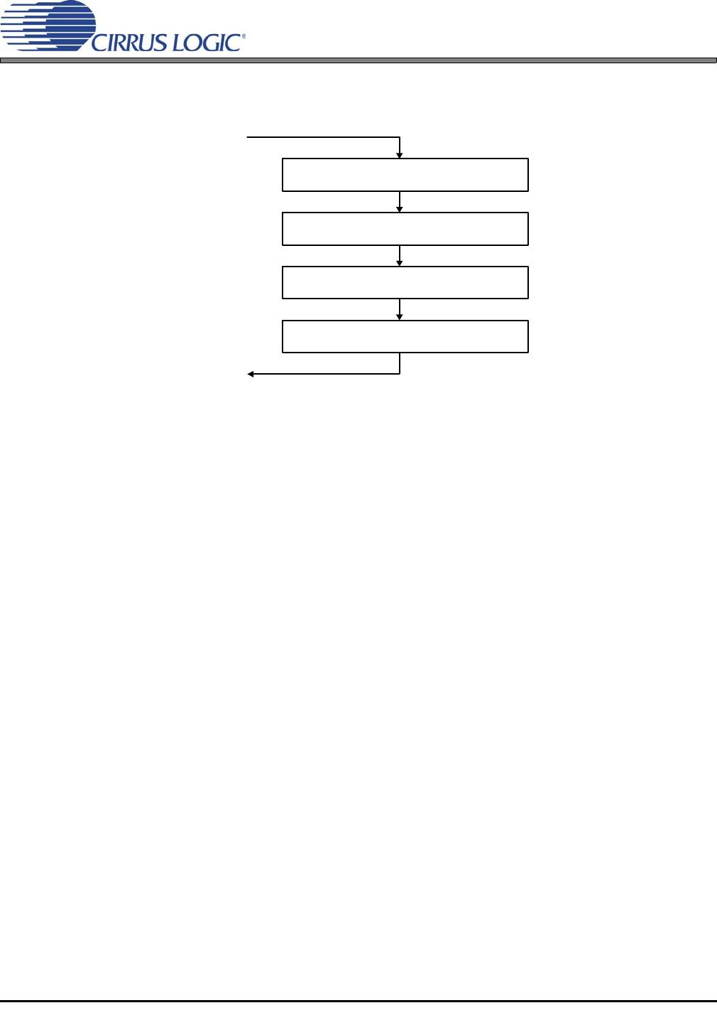
EtoFinterruptoccurs
Optionally set E to F inhibit
If set, clear E to F inhibit
Return
Write E data
Wait for E to F transfer
Figure 18. Flowchart for Writing the E Buffer
38 DS580F6
CS8406
16.1.3.2 Two-Byte Mode
There are those applications in which the A and B channel status blocks will not be the same, and the user
is interested in accessing both blocks. In these situations, Two-Byte Mode should be used to access the E
buffer.
In this mode, a read will cause the CS8406 to output two bytes from its control port. The first byte out will
represent the A channel status data, and the 2nd byte will represent the B channel status data. Writing is
similar, in that two bytes must now be input to the CS8406's control port. The A channel status data is first;
B channel status data second.
16.2 AES3 User (U) Bit Management
The CS8406 U bit manager has two operating modes:
Mode 1. Transmit all zeros.
Mode 2. Block mode.
16.2.1 Mode 1: Transmit All Zeros
Mode 1 causes only zeros to be transmitted in the output U data, regardless of E buffer contents. This
mode is intended for the user who wants the output U channel to contain no data.
16.2.2 Mode 2: Block Mode
Mode 2 is very similar to the scheme used to control the C bits. Entire blocks of U data are buffered using
2 block-sized RAMs to perform the buffering. The user has access to the first buffer, denoted the E buffer,
through the control port. It is the only mode in which the user can merge his own U data into the transmit-
ted AES3 data stream. The U buffer access only operates in Two-Byte Mode, since there is no concept
of A and B blocks for user data. The ar rangement of the data is as followings: Bit15[A7] Bit14[B7]
Bit13[A6] Bit12 [B6]...Bit1 [A0] Bit0[B0]. The arrangement of the data in the each byte is that the MSB is
the first transmitted bit. The bit for the A subframe is followed by the bit for the B subframe.
DS580F6 39
CS8406
17.REVISION HISTORY
Release Date Changes
F3 July 2005
-Updated Packaging Information to include Lead Free devices and updated “Table of
Contents” on page 2.
F4 April 2006
-Removed references to “Autoincrement” feature in “Control Port Description” on
page 16. Indicated that the MAP will always increment.
-Corrected definition of pin 5 in “Pin Description - Software Mode” on page 25.
F5 October 2009
- Added QFN package option to “General Description” on page 1, “Package Dimen-
sions” on page 32, and “Ordering Information” on page 34.
- Added QFN pin-out drawing and thermal pad description to “Pin Description - Software
Mode” on page 25 and “Pin Description - Hardware Mode” on page 30.
- Added QFN thermal pad guidelines to “Power Supply, Grounding, and PCB layout” on
page 33.
F6 Aug 2012
Removed QFN package options listed in F5 (reverted content to F4 release).
Contacting Cirrus Logic Support
For all product questions and inquiries, contact a Cirrus Logic Sales Representative.
To find the one nearest to you, go to
www.cirrus.com
IIMPORTANT NOTICE
Cirrus Logic, Inc. and its subsidiaries ("Cirrus") believe that the information contained in this document is accurate and reliable. However, the information is subject
to change without notice and is provided "AS IS" without warranty of any kind (express or implied). Customers are advised to obtain the latest version of relevant
information to verify, before placing orders, that information being relied on is current and complete. All products are sold subject to the terms and conditions of sale
supplied at the time of order acknowledgment, including those pertaining to warranty, indemnification, and limitation of liability. No responsibility is assumed by Cirrus
for the use of this information, including use of this information as the basis for manufacture or sale of any items, or for infringement of patents or other rights of third
parties. This document is the property of Cirrus and by furnishing this information, Cirrus grants no license, express or implied under any patents, mask work rights,
copyrights, trademarks, trade secrets or other intellectual property rights. Cirrus owns the copyrights associated with the information contained herein and gives con-
sent for copies to be made of the information only for use within your organization with respect to Cirrus integrated circuits or other products of Cirrus. This consent
does not extend to other copying such as copying for general distribution, advertising or promotional purposes, or for creating any work for resale.
CERTAIN APPLICATIONS USING SEMICONDUCTOR PRODUCTS MAY INVOLVE POTENTIAL RISKS OF DEATH, PERSONAL INJURY, OR SEVERE PROP-
ERTY OR ENVIRONMENTAL DAMAGE (“CRITICAL APPLICATIONS”). CIRRUS PRODUCTS ARE NOT DESIGNED, AUTHORIZED OR WARRANTED FOR USE
IN AIRCRAFT SYSTEMS, MILITARY APPLICATIONS, PRODUCTS SURGICALLY IMPLANTED INTO THE BODY, AUTOMOTIVE SAFETY OR SECURITY DE-
VICES, LIFE SUPPORT PR ODUCTS OR OTHER CRITICAL APPLICATIONS. INCLUSION OF CIRRUS PRODUCTS IN SUCH APPLICATIONS IS UNDER-
STOOD TO BE F ULLY AT THE CUSTOMER’S RISK AND CI RRUS DISCLAIMS AND MAKES NO WARRANTY, EXPRESS, STATUTORY OR I MPLIED,
INCLUDING THE IMPLIED WARRANTIES OF MERCHANTABILITY AND FITNESS FOR PARTICULAR PURPOSE, WITH REGARD TO ANY CIRRUS PRODUCT
THAT IS USED IN SUCH A MANNER. IF THE CUSTOMER OR CUSTOMER’S CUSTOMER USES OR PERMITS THE USE OF CIRRUS PRODUCTS IN CRITICAL
APPLICATIONS, CUSTOMER AGREES, BY SUCH USE, TO FULLY INDEMNIFY CIRRUS, ITS OFFICERS, DIRECTORS, EMPLOYEES, DISTRIBUTORS AND
OTHER AGENTS FROM ANY AND ALL LIABILITY, INCLUDING ATTORNEYS’ FEES AND COSTS, THAT MAY RESULT FROM OR ARISE IN CONNECTION
WITH THESE USES.
Cirrus Logic, Cirrus, and the Cirrus Logic logo designs are trademarks of Cirrus Logic, Inc. All other brand and product names in this document may be trademarks
or service marks of their respective owners.
I²C is a registered trademark of Philips Semiconductor.
SPI is a trademark of Motorola, Inc.

CS8406-DSZ

Mfr. #:
Manufacturer:
Cirrus Logic
Description:
Audio Transmitters, Receivers, Transceivers 192kHz Digital Audio Transmitter
Lifecycle:
New from this manufacturer.
Delivery:
DHL FedEx Ups TNT EMS
Payment:
T/T Paypal Visa MoneyGram Western Union