S70FL01GS
1 Gbit (128 Mbyte) 3.0V SPI Flash
Cypress Semiconductor Corporation 198 Champion Court San Jose, CA 95134-1709 408-943-2600
Document Number: 001-98295 Rev. *L Revised April 05, 2017
Features
CMOS 3.0V Core
Serial Peripheral Interface (SPI) with Multi-I/O
SPI Clock polarity and phase modes 0 and 3
– Double Data Rate (DDR) option
– Extended Addressing: 32-bit address
Serial Command set and footprint compatible with
S25FL-A, S25FL-K, and S25FL-P SPI families
Multi I/O Command set and footprint compatible with
S25FL-P SPI family
READ Commands
Normal, Fast, Dual, Quad, Fast DDR, Dual DDR, Quad
DDR
AutoBoot – power up or reset and execute a Normal or
Quad read command automatically at a preselected
address
Common Flash Interface (CFI) data for configuration
information
Programming (1.5 Mbytes/s)
512-byte Page Programming buffer
Quad-Input Page Programming (QPP) for slow clock
systems
Erase (0.5 Mbytes/s)
Uniform 256-kbyte sectors
Cycling Endurance
100,000 Program-Erase Cycles, minimum
Data Retention
20 Year Data Retention, minimum
Security Features
One Time Program (OTP) array of 1024 bytes
Block Protection
Status Register bits to control protection against program
or erase of a contiguous range of sectors.
– Hardware and software control options
Advanced Sector Protection (ASP)
Individual sector protection controlled by boot code or
password
Cypress
®
65 nm MirrorBit
®
Technology with Eclipse
Architecture
Core Supply Voltage: 2.7V to 3.6V
I/O Supply Voltage: 1.65V to 3.6V
Temperature Range / Grade:
Industrial (40 °C to +85 °C)
Industrial Plus (40 °C to +105 °C)
Automotive, AEC-Q100 Grade 3 (40 °C to +85 °C)
Automotive, AEC-Q100 Grade 2 (40 °C to +105 °C)
Automotive, AEC-Q100 Grade 1 (40 °C to +125 °C)
Packages (all Pb-free)
16-lead SOIC (300 mils)
BGA-24, 8 6 mm
–5 5 ball (ZSA024) footprint
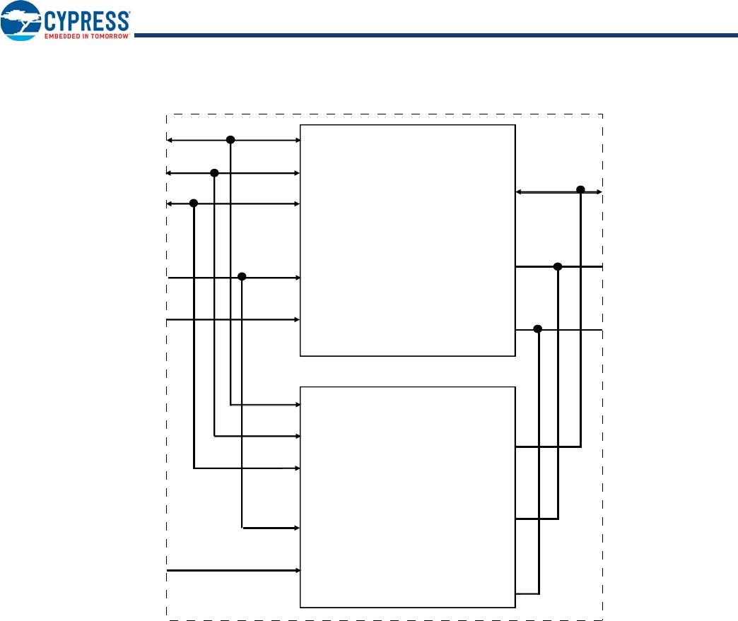
General Description
This document contains information for the S70FL01GS device, which is a dual die stack of two S25FL512S die. For detailed
specifications, refer to the discrete die datasheet provided in the Affected Documents/Related Documents table.
Affected Documents/Related Documents
Document Title Publication Number
S25FL512S 512 Mbit (64 Mbyte) 3.0V SPI Flash Memory Datasheet 001-98284
Document Number: 001-98295 Rev. *L Page 2 of 19
S70FL01GS
Contents
1. Block Diagram.............................................................. 3
2. Connection Diagrams.................................................. 4
3. Input/Output Summary................................................ 5
4. Device Operations ....................................................... 6
4.1 Programming ................................................................. 6
4.2 Simultaneous Die Operation.......................................... 6
4.3 Sequential Reads........................................................... 6
4.4 Sector/Bulk Erase .......................................................... 6
4.5 Status Registers............................................................. 6
4.6 Configuration Register................................................... 6
4.7 Bank Address Register .................................................. 6
4.8 Security and DDR Registers.......................................... 6
4.9 Block Protection............................................................. 6
5. Read Identification (RDID)........................................... 7
6. RESET#......................................................................... 7
7. Versatile I/O Power Supply (V
IO
)................................. 7
8. DC Characteristics....................................................... 8
9. AC Test Conditions...................................................... 9
10. SDR AC Characteristics ............................................. 10
10.1 DDR AC Characteristics ............................................... 11
10.2 Capacitance Characteristics ......................................... 11
11. Ordering Information.................................................. 12
11.1 Valid Combinations — Standard................................... 13
11.2 Valid Combinations — Automotive Grade /
AEC-Q100 .................................................................... 13
12. Other Resources......................................................... 14
12.1 Cypress Flash Memory Roadmap ................................ 14
12.2 Links to Software .......................................................... 14
12.3 Links to Application Notes............................................. 14
13. Physical Diagram........................................................ 15
13.1 SOIC 16 Lead, 300-mil Body Width.............................. 15
13.2 24-Ball BGA 8 x 6 mm (ZSA024).................................. 16
14. Revision History.......................................................... 17
Sales, Solutions, and Legal Information .......................... 19
Worldwide Sales and Design Support ...........................19
Products ........................................................................19
PSoC® Solutions ..........................................................19
Cypress Developer Community .....................................19
Technical Support .........................................................19
Document Number: 001-98295 Rev. *L Page 3 of 19
S70FL01GS
1. Block Diagram
SI/IO0
SI/IO0
WP#/IO2
WP#/IO2
SO/IO1
HOLD#/IO3
HOLD#/IO3
VSS
VSS
SCK
SCK
CS#1
CS#
VCC
VCC
SI/IO0
WP#/IO2
HOLD#/IO3
VSS
SCK
CS#2
CS#
VCC
SO/IO1
SO/IO1
FL512S
Flash
Memory
FL512S
Flash
Memory

S70FL01GSDSMFV010

Mfr. #:
Manufacturer:
Cypress Semiconductor
Description:
NOR Flash IC 1 Gb FLASH MEMORY
Lifecycle:
New from this manufacturer.
Delivery:
DHL FedEx Ups TNT EMS
Payment:
T/T Paypal Visa MoneyGram Western Union