Document Number: 001-98295 Rev. *L Page 7 of 19
S70FL01GS
5. Read Identification (RDID)
The Read Identification (RDID) command outputs the one-byte manufacturer identification, followed by the two-byte device
identification and the bytes for the Common Flash Interface (CFI) tables. Each die of the FL01GS dual die stack will have identical
identification data as the FL512S die, with the exception of the CFI data at byte 27h, as shown in Table 3.
6. RESET#
Note that the hardware RESET# input (pin 3 on the 16-pin SO package and ball A4 on the 5x5 BGA package) is bonded out and
active for the S70FL01GS device. For applications that do NOT require use of the RESET# pin, it is recommended to not use
RESET# for PCB routing channels that would cause the RESET# signal to be asserted Low (V
IL
). Doing so will cause the device to
reset to standby state. The RESET# signal has an internal pull-up resistor and may be left unconnected in the host system if not
used.
7. Versatile I/O Power Supply (V
IO
)
Note that the Versatile I/O (V
IO
) power supply (pin 14 on the 16-pin SO package and ball E4 on the 5x5 BGA package) is not
supported, and pin 14 and ball E4 are RFU (Reserved for Future Use) in the standard configuration of the S70FL01GS device.
Contact your local sales office to confirm availability with the V
IO
feature enabled.
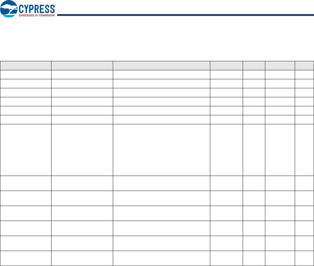
Table 3. Product Group CFI Device Geometry Definition
Byte Data Description
27h 1Bh Device Size = 2
N
byte
Document Number: 001-98295 Rev. *L Page 8 of 19
S70FL01GS
8. DC Characteristics
This section summarizes the DC Characteristics of the device.
Notes:
1. Typical values are at T
AI
= 25°C and V
CC
= 3V.
2. Output switching current is not included.
3. Bulk Erase current is for both die erasing simultaneously.
Table 4. DC Characteristics
Symbol Parameter Test Conditions Min Typ (1) Max Unit
V
IL
Input Low Voltage -0.5 0.2 x V
CC
V
V
IH
Input High Voltage 0.7 x V
CC
V
CC
+ 0.4 V
V
OL
Output Low Voltage I
OL
= 1.6 mA, V
CC
= V
CC
min  0.15 x V
CC
V
V
OH
Output High Voltage I
OH
= –0.1 mA 0.85 x V
CC
V
I
LI
Input Leakage Current V
CC
= V
CC
Max, V
IN
= V
IH
or V
IL
±4 µA
I
LO
Output Leakage Current V
CC
= V
CC
Max, V
IN
= V
IH
or V
IL
±4 µA
I
CC1
Active Power Supply
Current (READ)
Serial SDR @ 50 MHz
Serial SDR @ 133 MHz
Quad SDR @ 80 MHz
Quad SDR @ 104 MHz
Quad DDR @ 66 MHz
Quad DDR @ 80 MHz
Outputs unconnected during read data
return (2)
18
36
50
61
75
90
mA
I
CC2
Active Power Supply
Current (Page Program)
CS# = V
CC
100 mA
I
CC3
Active Power Supply
Current (WRR)
CS# = V
CC
100 mA
I
CC4
Active Power Supply
Current (SE)
CS# = V
CC
100 mA
I
CC5
Active Power Supply
Current (BE) (3)
CS# = V
CC
200 mA
I
SB
(Industrial) Standby Current
RESET#, CS# = V
CC
; SI, SCK = V
CC
or
V
SS
, Industrial Temp
70 200 µA
I
SB
(Industrial Plus) Standby Current
RESET#, CS# = V
CC
; SI, SCK = V
CC
or
V
SS
, Industrial Plus Temp
70 300 µA
Document Number: 001-98295 Rev. *L Page 9 of 19
S70FL01GS
9. AC Test Conditions
Figure 3. Input, Output, and Timing Reference Levels
Figure 4. Test Setup
Notes:
1. Output High-Z is defined as the point where data is no longer driven.
2. Input slew rate: 1.5 V/ns.
3. AC characteristics tables assume clock and data signals have the same slew rate (slope).
4. DDR Operation.
Table 5. AC Measurement Conditions
Symbol Parameter Min Max Unit
C
L
Load Capacitance
30
15 (4)
pF
Input Rise and Fall Times 2.4 ns
Input Pulse Voltage 0.2 x V
CC
to 0.8 V
CC
V
Input Timing Ref Voltage 0.5 V
CC
V
Output Timing Ref Voltage 0.5 V
CC
V
V
CC
+ 0.4V
0.7 x V
CC
0.2 x V
CC
- 0.5V
Timing Reference Level
0.5 x V
CC
0.85 x V
CC
0.15 x V
CC
Input Levels
Output Levels

S70FL01GSDSMFV010

Mfr. #:
Manufacturer:
Cypress Semiconductor
Description:
NOR Flash IC 1 Gb FLASH MEMORY
Lifecycle:
New from this manufacturer.
Delivery:
DHL FedEx Ups TNT EMS
Payment:
T/T Paypal Visa MoneyGram Western Union