Document Number: 001-98295 Rev. *L Page 10 of 19
S70FL01GS
10. SDR AC Characteristics
Notes:
1. Only applicable as a constraint for WRR instruction when SRWD is set to a 1.
2. Full V
CC
range (2.7 - 3.6V) and CL = 30 pF.
3. Regulated V
CC
range (3.0 - 3.6V) and CL = 30 pF.
4. Regulated V
CC
range (3.0 - 3.6V) and CL = 15 pF.
5. ±10% duty cycle is supported for frequencies
50 MHz.
6. Maximum value only applies during Program/Erase Suspend/Resume commands.
7. When switching between die, a minimum time of t
CS
must be kept between the rising edge of one chip select and the falling edge of the other for operations and data
to be valid.
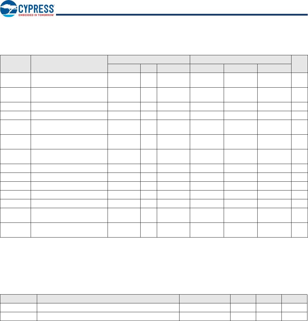
Table 6. SDR AC Characteristics (Single Die Package, V
CC
= 2.7V to 3.6V)
Symbol Parameter Min Typ Max Unit
F
SCK, R
SCK Clock Frequency for READ and 4READ instructions DC 50 MHz
F
SCK, C
SCK Clock Frequency for single commands (4) DC 133 MHz
F
SCK, C
SCK Clock Frequency for the following dual and quad commands:
DOR, 4DOR, QOR, 4QOR, DIOR, 4DIOR, QIOR, 4QIOR
DC
104 MHz
F
SCK, QPP
SCK Clock Frequency for the QPP, 4QPP commands DC 80 MHz
P
SCK
SCK Clock Period 1/ F
SCK
t
WH
, t
CH
Clock High Time (5) 45% P
SCK
ns
t
WL
, t
CL
Clock Low Time (5) 45% P
SCK
ns
t
CRT
, t
CLCH
Clock Rise Time (slew rate) 0.1 V/ns
t
CFT
, t
CHCL
Clock Fall Time (slew rate) 0.1 V/ns
t
CS
(7)
CS# High Time (Read Instructions)
CS# High Time (Program/Erase)
10
50
ns
t
CSS
CS# Active Setup Time (relative to SCK) 3 ns
t
CSH
CS# Active Hold Time (relative to SCK) 3 3000 (6) ns
t
SU
Data in Setup Time 1.5 ns
t
HD
Data in Hold Time 2 ns
t
V
Clock Low to Output Valid
8.0 (2)
7.65 (3)
6.5 (4)
ns
t
HO
Output Hold Time 2 ns
t
DIS
Output Disable Time 0 8 ns
t
WPS
WP# Setup Time 20 (1) ns
t
WPH
WP# Hold Time 100 (1) ns
t
HLCH
HOLD# Active Setup Time (relative to SCK) 3 ns
t
CHHH
HOLD# Active Hold Time (relative to SCK) 3 ns
t
HHCH
HOLD# Non-Active Setup Time (relative to SCK) 3 ns
t
CHHL
HOLD# Non-Active Hold Time (relative to SCK) 3 ns
t
HZ
HOLD# Enable to Output Invalid 8 ns
t
LZ
HOLD# Disable to Output Valid 8 ns
Document Number: 001-98295 Rev. *L Page 11 of 19
S70FL01GS
10.1 DDR AC Characteristics
Notes:
1. Regulated V
CC
range (3.0 - 3.6V) and CL =15 pF.
2. Maximum value only applies during Program/Erase Suspend/Resume commands.
10.2 Capacitance Characteristics
Note:
1. For more information on capacitance, please consult the IBIS models.
Table 7. DDR AC Characteristics 66 MHz and 80 MHz Operation
Symbol Parameter
66 MHz 80 MHz
Unit
Min Typ Max Min Typ Max
F
SCK, R
SCK Clock Frequency for DDR
READ instruction
DC 66 DC 80 MHz
P
SCK, R
SCK Clock Period for DDR
READ instruction
15
12.5 ns
t
WH
, t
CH
Clock High Time 45% P
SCK
45% P
SCK
ns
t
WL
, t
CL
Clock Low Time 45% P
SCK
45% P
SCK
ns
t
CS
CS# High Time (Read
Instructions)
10 10 ns
t
CSS
CS# Active Setup Time (relative
to SCK)
3
3 ns
t
CSH
CS# Active Hold Time (relative
to SCK)
3
3 ns
t
SU
IO in Setup Time 2 3000 (2) 1.5 3000 (2) ns
t
HD
IO in Hold Time 2 1.5 ns
t
V
Clock Low to Output Valid 0 6.5
(1) 6.5
(1) ns
t
HO
Output Hold Time 1.5 1.5 ns
t
DIS
Output Disable Time 8 8 ns
t
LZ
Clock to Output Low
Impedance
0 8 0 8 ns
t
IO_skew
First IO to last IO data valid
time
600 600 ps
Table 8. Capacitance
Parameter Test Conditions Min Max Unit
C
IN
Input Capacitance (applies to SCK, CS#1, CS#2, RESET#) 1 MHz 16 pF
C
OUT
Output Capacitance (applies to All I/O) 1 MHz 16 pF
Document Number: 001-98295 Rev. *L Page 12 of 19
S70FL01GS
11. Ordering Information
The ordering part number is formed by a valid combination of the following:
Notes:
1. EHPLC = Enhanced High Performance Latency Code table.
2. Uniform 256-kB sectors = All sectors are uniform 256-kB with a 512B programming buffer.
S70FL 01G S AG M F I 0 1 1
Packing Type (Note 1)
0 = Tray
1 = Tube
3 = 13” Tape and Reel
Model Number (Sector Type)
1 = Uniform 256-kB sectors
Model Number
(Latency Type, Package Details, RESET# support)
0 = EHPLC, SO footprint
C = EHPLC, 5 x 5 ball BGA footprint with RESET#
Temperature Range / Grade
I = Industrial (-40°C to + 85°C)
V = Industrial Plus (-40°C to +105°C)
A = Automotive, AEC-Q100 Grade 3 (-40°C to +85°C)
B = Automotive, AEC-Q100 Grade 2 (-40°C to +105°C)
M = Automotive, AEC-Q100 Grade 1(-40°C to +125°C)
Package Materials
F = Lead (Pb)-free
H = Low-Halogen, Lead (Pb)-free
Package Type
B = 24-ball BGA 8 x 6 mm package, 1.00 mm pitch
M = 16-pin SO package
Speed
AG = 133 MHz
DP = 66 MHz DDR
DS = 80 MHz DDR
Device Technology
S = 65 nm MirrorBit Process Technology
Density
01G = 1 Gbit
Device Family
S70FL
Cypress Stacked Memory 3.0V-Only, Serial Peripheral Interface (SPI) Flash Memory

S70FL01GSDSMFV010

Mfr. #:
Manufacturer:
Cypress Semiconductor
Description:
NOR Flash IC 1 Gb FLASH MEMORY
Lifecycle:
New from this manufacturer.
Delivery:
DHL FedEx Ups TNT EMS
Payment:
T/T Paypal Visa MoneyGram Western Union