LT6109-1/LT6109-2
11
610912fa
APPLICATIONS INFORMATION
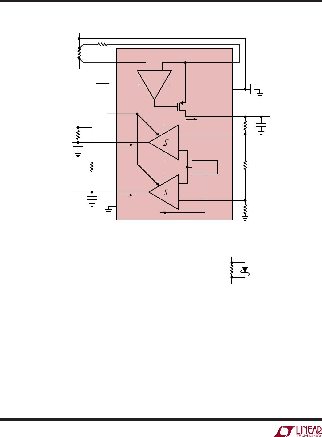
The output current can be transformed back into a voltage
by adding a resistor from OUTA to V
–
(typically ground).
The output voltage is then:
V
OUT
= V
–
+ I
OUTA
• R
OUT
where R
OUT
= R1 + R2 + R3 as shown in Figure 3.
Table 1. Example Gain Configurations
GAIN R
IN
R
OUT
V
SENSE
FOR V
OUT
= 5V I
OUTA
AT V
OUT
= 5V
20 499Ω 10k 250mV 500µA
50 200Ω 10k 100mV 500µA
100 100Ω 10k 50mV 500µA
Useful Equations
Input Voltage: V
SENSE
= I
SENSE
• R
SENSE
Voltage Gain:
V
OUT
V
SENSE
=
R
OUT
R
IN
Current Gain:
I
OUTA
I
SENSE
=
R
SENSE
R
IN
Note that V
SENSE(MAX)
can be exceeded without damag-
ing the amplifier, however, output accuracy will degrade
as V
SENSE
exceeds V
SENSE(MAX)
, resulting in increased
output current, I
OUTA
.
Selection of External Current Sense Resistor
The external sense resistor, R
SENSE
, has a significant effect
on the function of a current sensing system and must be
chosen with care.
First, the power dissipation in the resistor should be
considered. The measured load current will cause power
dissipation as well as a voltage drop in R
SENSE
. As a
result, the sense resistor should be as small as possible
while still providing the input dynamic range required by
the measurement. Note that the input dynamic range is
the difference between the maximum input signal and the
minimum accurately reproduced signal, and is limited
primarily by input DC offset of the internal sense ampli-
fier of the LT6109. To ensure the specified performance,
R
SENSE
should be small enough that V
SENSE
does not
exceed V
SENSE(MAX)
under peak load conditions. As an
example, an application may require the maximum sense
voltage be 100mV. If this application is expected to draw
2A at peak load, R
SENSE
should be set to 50mΩ.
Once the maximum R
SENSE
value is determined, the mini-
mum sense resistor value will be set by the resolution or
dynamic range required. The minimum signal that can be
accurately represented by this sense amplifier is limited by
the input offset. As an example, the LT6109 has a maximum
input offset of 125µV. If the minimum current is 20mA, a
sense resistor of 6.25mΩ will set V
SENSE
to 125µV. This is
the same value as the input offset. A larger sense resistor
will reduce the error due to offset by increasing the sense
voltage for a given load current. Choosing a 50mΩ R
SENSE
will maximize the dynamic range and provide a system
that has 100mV across the sense resistor at peak load
(2A), while input offset causes an error equivalent to only
2.5mA of load current.
In the previous example, the peak dissipation in R
SENSE
is 200mW. If a 5mΩ sense resistor is employed, then
the effective current error is 25mA, while the peak sense
voltage is reduced to 10mV at 2A, dissipating only 20mW.
The low offset and corresponding large dynamic range of
the LT6109 make it more flexible than other solutions in this
respect. The 125µV maximum offset gives 72dB of dynamic
range for a sense voltage that is limited to 500mV max.
Sense Resistor Connection
Kelvin connection of the SENSEHI and SENSELO inputs
to the sense resistor should be used in all but the lowest
power applications. Solder connections and PC board
interconnections that carry high currents can cause sig-
nificant error in measurement due to their relatively large
resistances. One 10mm × 10mm square trace of 1oz copper
is approximately 0.5mΩ. A 1mV error can be caused by as
little as 2A flowing through this small interconnect. This
will cause a 1% error for a full-scale V
SENSE
of 100mV.
A 10A load current in the same interconnect will cause
a 5% error for the same 100mV signal. By isolating the
sense traces from the high current paths, this error can
be reduced by orders of magnitude. A sense resistor with
integrated Kelvin sense terminals will give the best results.
Figure 3 illustrates the recommended method for connect-
ing the SENSEHI and SENSELO pins to the sense resistor.