LT6109-1/LT6109-2
13
610912fa
APPLICATIONS INFORMATION
In this case, the only error is due to external resistor
mismatch, which provides an error in gain only. However,
offset voltage, input bias current and finite gain in the
amplifier can cause additional errors:
Output Voltage Error, V
OUT(VOS)
, Due to the Amplifier
DC Offset Voltage, V
OS
V
OUT(VOS)
= V
OS
R
OUT
R
IN
The DC offset voltage of the amplifier adds directly to the
value of the sense voltage, V
SENSE
. As V
SENSE
is increased,
accuracy improves. This is the dominant error of the system
and it limits the available dynamic range.
Output Voltage Error, V
OUT(IBIAS)
, Due to the Bias
Currents I
B
+
and I
B
The amplifier bias current I
B
+
flows into the SENSELO pin
while I
B
flows into the SENSEHI pin. The error due to I
B
is the following:
V
OUT(IBIAS)
= R
OUT
I
B
+
R
SENSE
R
IN
I
B
Since I
B
+
≈ I
B
= I
BIAS
, if R
SENSE
<< R
IN
then,
V
OUT(IBIAS)
= –R
OUT
(I
BIAS
)
It is useful to refer the error to the input:
V
VIN(IBIAS)
= –R
IN
(I
BIAS
)
For instance, if I
BIAS
is 100nA and R
IN
is 1k, the input re-
ferred error is 100µV. This error becomes less significant
as the value of R
IN
decreases. The bias current error can
be reduced if an external resistor, R
IN
+
, is connected as
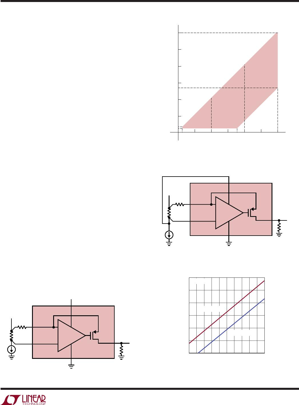
shown in Figure 5, the error is then reduced to:
V
OUT(IBIAS)
= ±R
OUT
• I
OS
; I
OS
= I
B
+
– I
B
Minimizing low current errors will maximize the dynamic
range of the circuit.
should be taken to place R
IN
and R
OUT
such that the gain
error due to the thermal gradient is minimized.
Selection of External Output Gain Resistor, R
OUT
The output resistor, R
OUT
, determines how the output cur-
rent is converted to voltage. V
OUT
is simply I
OUTA
R
OUT
.
Typically, R
OUT
is a combination of resistors configured
as a resistor divider which has voltage taps going to the
comparator inputs to set the comparator thresholds.
In choosing an output resistor, the maximum output volt-
age must first be considered. If the subsequent circuit is a
buffer or ADC with limited input range, then R
OUT
must be
chosen so that I
OUTA(MAX)
R
OUT
is less than the allowed
maximum input range of this circuit.
In addition, the output impedance is determined by R
OUT
.
If another circuit is being driven, then the input impedance
of that circuit must be considered. If the subsequent circuit
has high enough input impedance, then almost any use-
ful output impedance will be acceptable. However, if the
subsequent circuit has relatively low input impedance, or
draws spikes of current such as an ADC load, then a lower
output impedance may be required to preserve the accuracy
of the output. More information can be found in the Output
Filtering section. As an example, if the input impedance of
the driven circuit, R
IN(DRIVEN)
, is 100 times R
OUT
, then the
accuracy of V
OUT
will be reduced by 1% since:
V
OUT
= I
OUTA
R
OUT
R
IN(DRIVEN)
R
OUT
+R
IN(DRIVEN)
= I
OUTA
R
OUT
100
101
= 0.99 I
OUTA
R
OUT
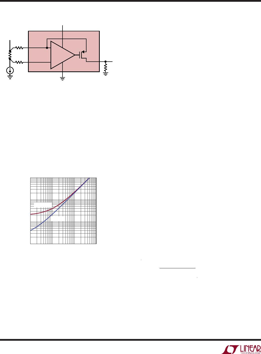
Amplifier Error Sources
The current sense system uses an amplifier and resistors
to apply gain and level-shift the result. Consequently, the
output is dependent on the characteristics of the amplifier,
such as gain error and input offset, as well as the matching
of the external resistors.
Ideally, the circuit output is:
V
OUT
= V
SENSE
R
OUT
R
IN
; V
SENSE
= R
SENSE
I
SENSE
LT6109-1/LT6109-2
14
610912fa
APPLICATIONS INFORMATION
There is also power dissipated due to the quiescent power
supply current:
P
S
= I
S
• V
+
The comparator output current flows into the comparator
output pin and out of the V
pin. The power dissipated in
the LT6109 due to each comparator is often insignificant
and can be calculated as follows:
P
OUTC1,C2
= (V
OUTC1,C2
– V
) • I
OUTC1,C2
The total power dissipated is the sum of these
dissipations:
P
TOTAL
= P
OUTA
+ P
OUTC1
+ P
OUTC2
+ P
S
At maximum supply and maximum output currents, the
total power dissipation can exceed 100mW. This will
cause significant heating of the LT6109 die. In order to
prevent damage to the LT6109, the maximum expected
dissipation in each application should be calculated. This
number can be multiplied by the θ
JA
value, 160°C/W, to
find the maximum expected die temperature. Proper heat
sinking and thermal relief should be used to ensure that
the die temperature does not exceed the maximum rating.
Output Filtering
The AC output voltage, V
OUT
, is simply I
OUTA
Z
OUT
. This
makes filtering straightforward. Any circuit may be used
which generates the required Z
OUT
to get the desired filter
response. For example, a capacitor in parallel with R
OUT
will give a lowpass response. This will reduce noise at the
output, and may also be useful as a charge reservoir to
keep the output steady while driving a switching circuit
such as a MUX or ADC. This output capacitor in parallel
with R
OUT
will create an output pole at:
f
3dB
=
1
2 π R
OUT
C
L
SENSELO, SENSEHI Range
The difference between V
BATT
(see Figure 7) and V
+
, as
well as the maximum value of V
SENSE
, must be considered
to ensure that the SENSELO pin doesn’t exceed the range
listed in the Electrical Characteristics table. The SENSELO
and SENSEHI pins of the LT6109 can function from 0.2V
Figure 6. Gain Error vs Resistor Tolerance
SENSEHI
LT6109
I
SENSE
R
SENSE
V
+
9
V
5
V
+
R
IN
V
BATT
SENSELO
10
1
OUTA 8
610912 F05
R
OUT
V
OUT
R
IN
+
+
Figure 5. R
IN
+
Reduces Error Due to I
B
Output Voltage Error, V
OUT(GAIN ERROR)
, Due to
External Resistors
The LT6109 exhibits a very low gain error. As a result,
the gain error is only significant when low tolerance
resistors are used to set the gain. Note the gain error is
systematically negative. For instance, if 0.1% resistors
are used for R
IN
and R
OUT
then the resulting worst-case
gain error is –0.4% with R
IN
= 100Ω. Figure 6 is a graph
of the maximum gain error which can be expected versus
the external resistor tolerance.
Output Current Limitations Due to Power Dissipation
The LT6109 can deliver a continuous current of 1mA to the
OUTA pin. This current flows through R
IN
and enters the
current sense amplifier via the SENSEHI pin. The power
dissipated in the LT6109 due to the output signal is:
P
OUT
= (V
SENSEHI
– V
OUTA
) • I
OUTA
Since V
SENSEHI
≈ V
+
, P
OUTA
≈ (V
+
– V
OUTA
) • I
OUTA
RESISTOR TOLERANCE (%)
0.01
0.01
RESULTING GAIN ERROR (%)
0.1
1
10
0.1 1 10
610912 F06
R
IN
= 100Ω
R
IN
= 1k
LT6109-1/LT6109-2
15
610912fa
above the positive supply to 33V below it. These operat-
ing voltages are limited by internal diode clamps shown
in Figures 1 and 2. On supplies less than 35.5V, the lower
range is limited by V
+ 2.5V. This allows the monitored
supply, V
BATT
, to be separate from the LT6109 positive
supply as shown in Figure 7. Figure 8 shows the range of
operating voltages for the SENSELO and SENSEHI inputs,
for different supply voltage inputs (V
+
). The SENSELO and
SENSEHI range has been designed to allow the LT6109 to
monitor its own supply current (in addition to the load),
as long as V
SENSE
is less than 200mV. This is shown in
Figure 9.
Minimum Output Voltage
The output of the LT6109 current sense amplifier can
produce a non-zero output voltage when the sense voltage
is zero. This is a result of the sense amplifier V
OS
being
forced across R
IN
as discussed in the Output Voltage Er-
ror, V
OUT(VOS)
section. Figure 10 shows the effect of the
input offset voltage on the transfer function for parts at
the V
OS
limits. With a negative offset voltage, zero input
sense voltage produces an output voltage. With a positive
offset voltage, the output voltage is zero until the input
sense voltage exceeds the input offset voltage. Neglect-
ing V
OS
, the output circuit is not limited by saturation of
pull-down circuitry and can reach 0V.
Response Time
The LT6109 amplifier is designed to exhibit fast response
to inputs for the purpose of circuit protection or current
monitoring. This response time will be affected by the
external components in two ways, delay and speed.
APPLICATIONS INFORMATION
Figure 9. LT6109 Supply Current Monitored with Load
Figure 7. V
+
Powered Separately from Load Supply (V
BATT
)
Figure 8. Allowable SENSELO, SENSEHI Voltage Range
SENSEHI
LT6109
I
SENSE
R
SENSE
V
+
9
V
5
V
+
R
IN
V
BATT
SENSELO
10
1
OUTA 8
610912 F07
R
OUT
V
OUT
+
60
50
40
30
20
20.2V
40.2V
10
27
ALLOWABLE OPERATING VOLTAGES ON
SENSELO AND SENSEHI INPUTS (V)
2.8V
2.5V
2.7 10 20 30 35.5 40 50
V
+
(V)
60
610912 F08
VALID SENSELO/
SENSEHI RANGE
SENSEHI
LT6109
I
SENSE
R
SENSE
V
+
9
V
5
R
IN
V
BATT
SENSELO
10
1
OUTA 8
610912 F09
R
OUT
V
OUT
+
Figure 10. Amplifier Output Voltage vs Input Sense Voltage
INPUT SENSE VOLTAGE (µV)
0
OUTPUT VOLTAGE (mV)
40
80
120
20
60
100
200 400 600 800
610912 F10
10001000 300 500 700 900
V
OS
= –125µV
V
OS
= 125µV
G = 100

LT6109AIMS-2#PBF

Mfr. #:
Manufacturer:
Analog Devices Inc.
Description:
Current Sense Amplifiers Current Sense Amp with Reference and Comparators
Lifecycle:
New from this manufacturer.
Delivery:
DHL FedEx Ups TNT EMS
Payment:
T/T Paypal Visa MoneyGram Western Union