LT6109-1/LT6109-2
7
610912fa
Performance characteristics taken at T
A
= 25°C,
V
+
= 12V, V
PULLUP
= V
+
, V
EN/RST
= 2.7V, R
IN
= 100Ω, R
OUT
= R1 + R2 + R3 = 10k, gain = 100, R
C
= 25.5k, C
L
= C
LC
= 2pF, unless
otherwise noted. (See Figure 3)
Hysteresis Distribution
Hysteresis vs Temperature
Hysteresis vs Supply Voltage
Comparator Input Bias Current
vs Input Voltage
Comparator Input Bias Current
vs Input Voltage
Comparator Threshold
Distribution
Comparator Threshold
vs Temperature
EN/RST Current vs Voltage
Comparator Output Low Voltage
vs Output Sink Current
COMPARATOR INPUT VOLTAGE (V)
–20
COMPARATOR INPUT BIAS CURRENT (nA)
–10
0
10
–15
–5
5
20 40
610912 G25
600
125°C
25°C
–40°C
COMPARATOR INPUT VOLTAGE (V)
–20
COMPARATOR INPUT BIAS CURRENT (nA)
–10
0
10
–15
–5
5
0.2 0.4 0.6 0.8
610912 G26
1.00
125°C
25°C
–40°C
0
0
V
OL
OUTC1, OUTC2 (V)
0.25
0.50
0.75
1.00
1
I
OUTC
(mA)
2
610912 G27
3
125°C
25°C
–40°C
TYPICAL PERFORMANCE CHARACTERISTICS
TEMPERATURE (°C)
–40 –25
COMPARATOR THRESHOLD (mV)
398
400
402
50
110
610912 G20
396
394
392
–10 5 20 35 80
65
125
95
404
406
408
5 TYPICAL PARTS
COMPARATOR HYSTERESIS (mV)
3.0
0
PERCENTAGE OF UNITS (%)
5
10
15
20
30
–40°C 25°C 125°C
4.6
6.2 7.7 9.3 10.9 12.5 14.1
610912 G21
15.7 17.3
25
V
+
(V)
0
14
12
10
8
6
4
2
0
30 50
610912 G23
10 20
40 60
COMPARATOR HYSTERESIS (mV)
5 TYPICAL PARTS
EN/RST VOLTAGE (V)
0
–250
EN/RST CURRENT (nA)
–200
–150
–100
–50
50
10
20 30 40
610912 G24
50 60
0
COMPARATOR THRESHOLD (mV)
0
PERCENTAGE OF UNITS (%)
5
15
20
25
399.2 404
610912 G19
10
396 397.6
400.8
402.8
TEMPERATURE (°C)
–40
COMPARATOR HYSTERESIS (mV)
20
18
16
14
12
10
8
6
4
0
2
80
610912 G22
–10 20 50 12511065–25 5 35 95
LT6109-1/LT6109-2
8
610912fa
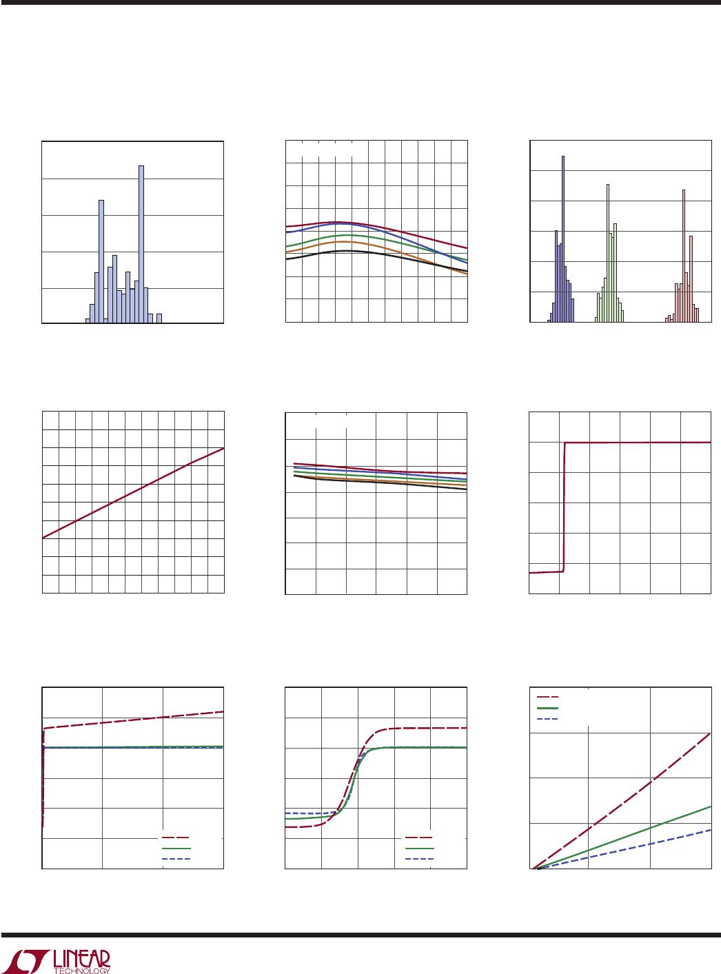
Comparator Rise/Fall Time
vs Pull-Up Resistor
Comparator Step Response
(5mV INC1 Overdrive)
Comparator Step Response
(100mV INC1 Overdrive)
Comparator Reset Response
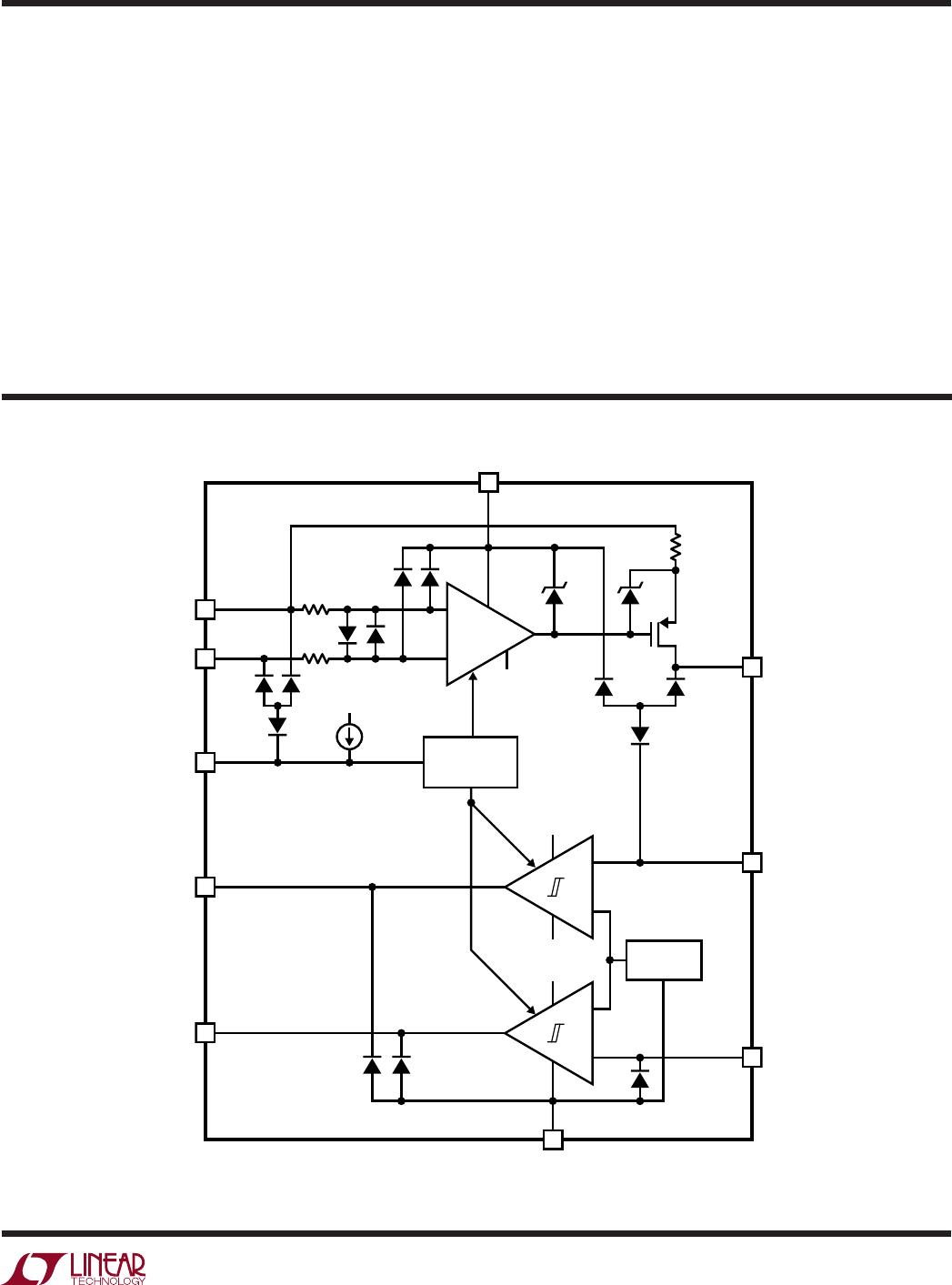
SENSELO (Pin 1): Sense Amplifier Input. This pin must
be tied to the load end of the sense resistor.
EN/RST (Pin 2): Enable and Latch Reset Input. When the
EN/RST pin is pulled high the LT6109 is enabled. When the
EN/RST pin is pulled low for longer than typically 40µs,
the LT6109 will enter the shutdown mode. Pulsing this pin
low for between 2µs and 15µs will reset the comparators
of the LT6109.
Comparator Propagation Delay
vs Input Overdrive
PIN FUNCTIONS
OUTC2 (Pin 3): Open-Drain Comparator 2 Output. Off-
state voltage may be as high as 60V above V
, regardless
of V
+
used.
OUTC1 (Pin 4):
Open-Drain Comparator 1 Output. Off-
state voltage may be as high as 60V above V
, regardless
of V
+
used.
V
(Pin 5): Negative Supply Pin. This pin is normally con-
nected to ground.
Comparator Output Leakage
Current vs Pull-Up Voltage
COMPARATOR OUTPUT PULL-UP VOLTAGE (V)
0
–2
OUTC1, OUTC2 LEAKAGE CURRENT (nA)
3
8
13
18
23
125°C
10
20 30 40
610912 G28
50 60
–40°C AND 25°C
R
C
PULL-UP RESISTOR (kΩ)
1
10
RISE/FALL TIME (ns)
100
1000
10000
10 100 1000
610912 G30
RISE TIME
FALL TIME
V
OH
= 0.9 • V
PULLUP
V
OL
= 0.1 • V
PULLUP
100mV INC1 OVERDRIVE
C
L
= 2pF
V
INC
0.5V/DIV
0V
V
OUTC
2V/DIV
0V
V
EN/RST
5V/DIV
0V
610912 G31
5µs/DIV
0V
V
INC
0.5V/DIV
V
OUTC
2V/DIV
V
EN/RST
5V/DIV
0V
0V
610912 G32
5µs/DIV
0V
V
OUTC
5V/DIV
V
EN/RST
2V/DIV
0V
5µs/DIV
610912 G33
Performance characteristics taken at T
A
= 25°C,
V
+
= 12V, V
PULLUP
= V
+
, V
EN/RST
= 2.7V, R
IN
= 100Ω, R
OUT
= R1 + R2 + R3 = 10k, gain = 100, R
C
= 25.5k, C
L
= C
LC
= 2pF, unless
otherwise noted. (See Figure 3)
TYPICAL PERFORMANCE CHARACTERISTICS
COMPARATOR INPUT OVERDRIVE (mV)
0
COMPARATOR PROPAGATION DELAY (µs)
3.0
4.0
5.0
160
610912 G29
2.0
1.0
2.5
3.5
4.5
1.5
0.5
0
40
80
120
200
H TO L
L TO H
LT6109-1/LT6109-2
9
610912fa
PIN FUNCTIONS
INC1 (Pin 6): This is the inverting input of comparator 1.
The second input of this comparator is internally connected
to the 400mV reference.
INC2 (Pin 7): This is the input of comparator 2. For the
LT6109-1 this is the noninverting input of comparator 2.
For the LT6109-2 this is the inverting input of compara-
tor2. The second input of each of these comparators is
internally connected to the 400mV reference.
OUTA (Pin 8): Current Output of the Sense Amplifier. This
pin will source a current that is equal to the sense voltage
divided by the external gain setting resistor, R
IN
.
V
+
(Pin 9): Positive Supply Pin. The V
+
pin can be con-
nected directly to either side of the sense resistor, R
SENSE
.
When V
+
is tied to the load end of the sense resistor, the
SENSEHI pin can go up to 0.2V above V
+
. Supply current
is drawn through this pin.
SENSEHI (Pin 10): Sense Amplifier Input. The internal
sense amplifier will drive SENSEHI to the same potential
as SENSELO. A resistor (typically R
IN
) tied from supply
to SENSEHI sets the output current, I
OUT
= V
SENSE
/R
IN
,
where V
SENSE
is the voltage developed across R
SENSE
.
BLOCK DIAGRAMS
Figure 1. LT6109-1 Block Diagram (Comparators with Opposing Polarity)
100Ω
OUTA
+
+
9
10
1
8
INC2
7
INC1
610912 F01
6
V
+
V
V
V
V
V
+
3k
V
+
3k
SENSEHI
LT6109-1
SENSELO
200nA
RESET
UNDERCURRENT FLAG
OVERCURRENT FLAG
2
EN/RST
3
OUTC2
4
OUTC1
34V 6V
ENABLE AND
RESET TIMING
+
V
V
+
5
400mV
REFERENCE

LT6109AIMS-2#PBF

Mfr. #:
Manufacturer:
Analog Devices Inc.
Description:
Current Sense Amplifiers Current Sense Amp with Reference and Comparators
Lifecycle:
New from this manufacturer.
Delivery:
DHL FedEx Ups TNT EMS
Payment:
T/T Paypal Visa MoneyGram Western Union