LTC4213
2
4213f
Bias Supply Voltage (V
CC
) ........................... –0.3V to 9V
Input Voltages
ON, SENSEP, SENSEN.............................–0.3V to 9V
I
SEL
.......................................... –0.3V to (V
CC
+ 0.3V)
Output Voltages
GATE .....................................................–0.3V to 15V
READY.....................................................– 0.3V to 9V
Operating Temperature Range
LTC4213C ............................................... 0°C to 70°C
LTC4213I............................................. –40°C to 85°C
Storage Temperature Range ................. –65°C to 150°C
Lead Temperature (Soldering, 10sec)................... 300°C
ORDER PART
NUMBER
DDB PART*
MARKING
T
JMAX
= 125°C, θ
JA
= 250°C/W
EXPOSED PAD (PIN 9)
PCB CONNECTION OPTIONAL
Consult LTC Marketing for parts specified with wider operating temperature ranges.
*The temperature grade is identified by a label on the shipping container.
LBHV
LTC4213CDDB
LTC4213IDDB
ABSOLUTE AXI U RATI GS
W
WW
U
PACKAGE/ORDER I FOR ATIO
UUW
(Note 1)
ELECTRICAL CHARACTERISTICS
The ● denotes the specifications which apply over the full operating
temperature range, otherwise specifications are at T
A
= 25°C. V
CC
= 5V, I
SEL
= 0 unless otherwise noted. (Note 2)
SYMBOL PARAMETER CONDITIONS MIN TYP MAX UNITS
V
CC
Bias Supply Voltage ● 2.3 6 V
V
SENSEP
SENSEP Voltage ● 06V
I
CC
V
CC
Supply Current ● 1.6 3 mA
V
CC(UVLR)
V
CC
Undervoltage Lockout Release V
CC
Rising ● 1.8 2.07 2.23 V
∆V
CC(UVHYST)
V
CC
Undervoltage Lockout Hysteresis ● 30 100 160 mV
I
SENSEP
SENSEP Input Current V
SENSEP
= V
SENSEN
= 5V, Normal Mode 15 40 80 µA
V
SENSEP
= V
SENSEN
= 0, Normal Mode –1 ±15 µA
I
SENSEN
SENSEN Input Current V
SENSEP
= V
SENSEN
= 5V, Normal Mode 15 40 80 µA
V
SENSEP
= V
SENSEN
= 0, Normal Mode –1 ±15 µA
V
SENSEP
= V
SENSEN
= 5V, 50 280 µA
Reset Mode or Fault Mode
V
CB
Circuit Breaker Trip Voltage I
SEL
= 0, V
SENSEP
= V
CC
● 22.5 25 27.5 mV
V
CB
= V
SENSEP
– V
SENSEN
I
SEL
= Floated, V
SENSEP
= V
CC
● 45 50 55 mV
I
SEL
= V
CC,
V
SENSEP
= V
CC
● 90 100 110 mV
V
CB(FAST)
Fast Circuit Breaker Trip Voltage I
SEL
= 0, V
SENSEP
= V
CC
● 63 100 115 mV
V
CB(FAST)
= V
SENSEP
– V
SENSEN
I
SEL
= Floated, V
SENSEP
= V
CC
● 126 175 200 mV
I
SEL
= V
CC,
V
SENSEP
= V
CC
● 252 325 371 mV
I
GATE(UP)
GATE Pin Pull Up Current V
GATE
= 0V ● –50 –100 –150 µA
I
GATE(DN)
GATE Pin Pull Down Current ∆V
SENSEP
– V
SENSEN
= 200mV, V
GATE
= 8V ● 10 40 mA
∆V
GSMAX
External N-Channel Gate Drive V
SENSEN
= 0, V
CC
≥ 2.97V, I
GATE
= –1µA ● 4.8 6.5 8 V
V
SENSEN
= 0, V
CC
= 2.3V, I
GATE
= –1µA ● 2.65 4.3 8 V
∆V
GSARM
V
GS
Voltage to Arm Circuit Breaker V
SENSEN
= 0, V
CC
≥ 2.97V ● 4.4 5.4 7.6 V
V
SENSEN
= 0, V
CC
= 2.3V ● 2.5 3.5 7 V
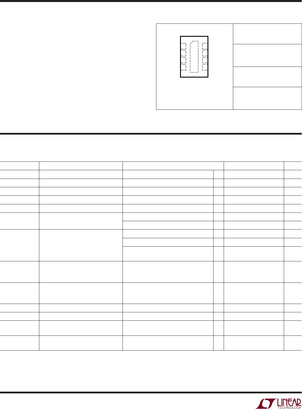
TOP VIEW
DDB PACKAGE
8-LEAD (3mm × 2mm) PLASTIC DFN
5
6
7
8
9
4
3
2
1READY
ON
I
SEL
GND
V
CC
SENSEP
SENSEN
GATE