LTC4213
7
4213f
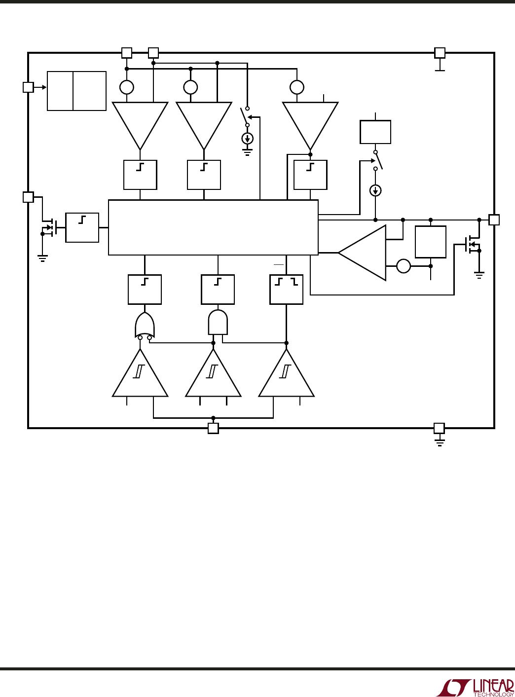
PI FU CTIO S
UUU
READY (Pin 1): READY Status Output. Open drain output
that goes high impedance when the external MOSFET is on
and the circuit breaker is armed. Otherwise this pin pulls
low.
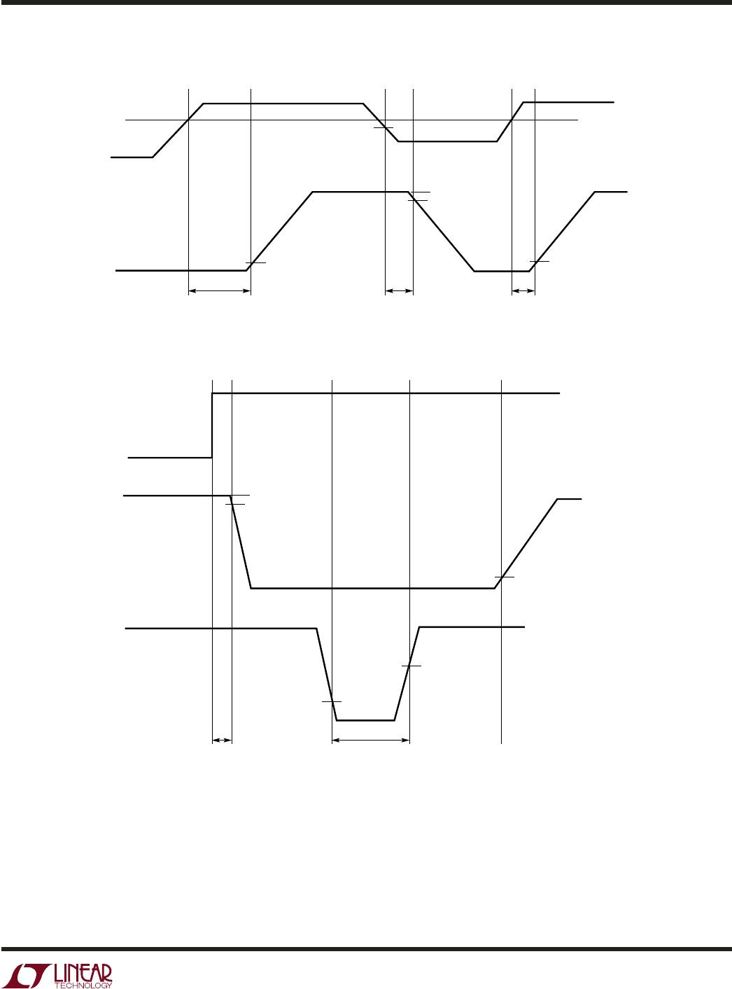
ON
(Pin 2): ON Control Input. The LTC4213 is in reset
mode when the ON pin is below 0.4V. When the ON pin
increases above 0.8V, the device starts up and the GATE
pulls up with a 100µA current source. When the ON pin
drops below 0.76V, the GATE pulls down. To reset a circuit
breaker fault, the ON pin must go below 0.4V.
I
SEL
(Pin 3): Threshold Select Input. With the I
SEL
pin
grounded, float or tied to V
CC
the V
CB
is set to 25mV, 50mV
or 100mV, respectively. The corresponding V
CB(FAST)
values are 100mV, 175mV and 325mV.
GND
(Pin 4): Device Ground.
GATE
(Pin 5): GATE Drive Output. An internal charge
pump supplies 100µA pull-up current to the gate of the
external N-channel MOSFET. Internal circuitry limits the
voltage between the GATE and SENSEN pins to a safe gate
drive voltage of less than 8V. When the circuit breaker
trips, the GATE pin abruptly pulls to GND.
SENSEN
(Pin 6): Circuit Breaker Negative Sense Input.
Connect this pin to the source of the external MOSFET.
During reset or fault mode, the SENSEN pin discharges the
output to ground with 280µA.
SENSEP
(Pin 7): Circuit Breaker Positive Sense Input.
Connect this pin to the drain of external N-channel MOSFET.
The circuit breaker trips when the voltage across SENSEP
and SENSEN exceeds V
CB
. The input common mode range
of the circuit breaker is from ground to V
CC
+ 0.2V when
V
CC
< 2.5V. For V
CC
≥ 2.5V, the input common mode range
is from ground to V
CC
+ 0.4V.
V
CC
(Pin 8): Bias Supply Voltage Input. Normal operation
is between 2.3V and 6V. An internal under-voltage lockout
circuit disables the device when V
CC
< 2.07V.
Exposed Pad (Pin 9): Exposed pad may be left open or
connected to device ground.