LTC4213
14
4213f
Operating temperature of 0° to 70°C.
R
DSON
@ 25°C = 100%
R
DSON
@ 0°C = 90%
R
DSON
@ 70°C = 120%
MOSFET resistance variation:
R
DSON(NOM)
= 15m • 0.82 = 12.3mΩ
R
DSON(MAX)
= 15m • 1.333 • 0.93 • 1.2 = 15m • 1.488
= 22.3mΩ
R
DSON(MIN)
= 15m • 0.667 • 0.80 • 0.90 = 15m • 0.480
= 7.2mΩ
V
CB
variation:
NOM V
CB
= 25mV = 100%
MIN V
CB
= 22.5mV = 90%
MAX V
CB
= 27.5mV = 110%
The current limits are:
I
LIMIT(NOM)
= 25mV/12.3mΩ = 2.03A
I
LIMIT(MIN)
= 22.5mV/22.3mΩ = 1.01A
I
LIMIT(MAX)
= 27.5mV/7.2mΩ = 3.82A
For proper operation, the minimum current limit must
exceed the circuit maximum operating load current with
margin. So this system is suitable for operating load
current up to 1A. From this calculation, we can start with
the general rule for MOSFET R
DSON
by assuming maxi-
mum operating load current is roughly half of the
I
LIMIT(NOM)
. Equation 7 shows the rule of thumb.
I
V
R
OPMAX
CB NOM
DSON NOM
=
()
()
•
()
2
7
Note that the R
DSON(NOM)
is at the LTC4213 nominal
operating ∆V
GSMAX
rather than at typical vendor spec.
Table 1 gives the nominal operating ∆V
GSMAX
at the
various operating V
CC
. From this table users can refer to
the MOSFET’s data sheet to obtain the R
DSON(NOM)
value.
Table 1. Nominal Operating ∆V
GSMAX
for Typical Bias
Supply Voltage
V
CC
(V) ∆V
GSMAX
(V)
2.3 4.3
2.5 5.0
2.7 5.6
3.0 6.5
3.3 7.0
5.0 7.0
6.0 7.0
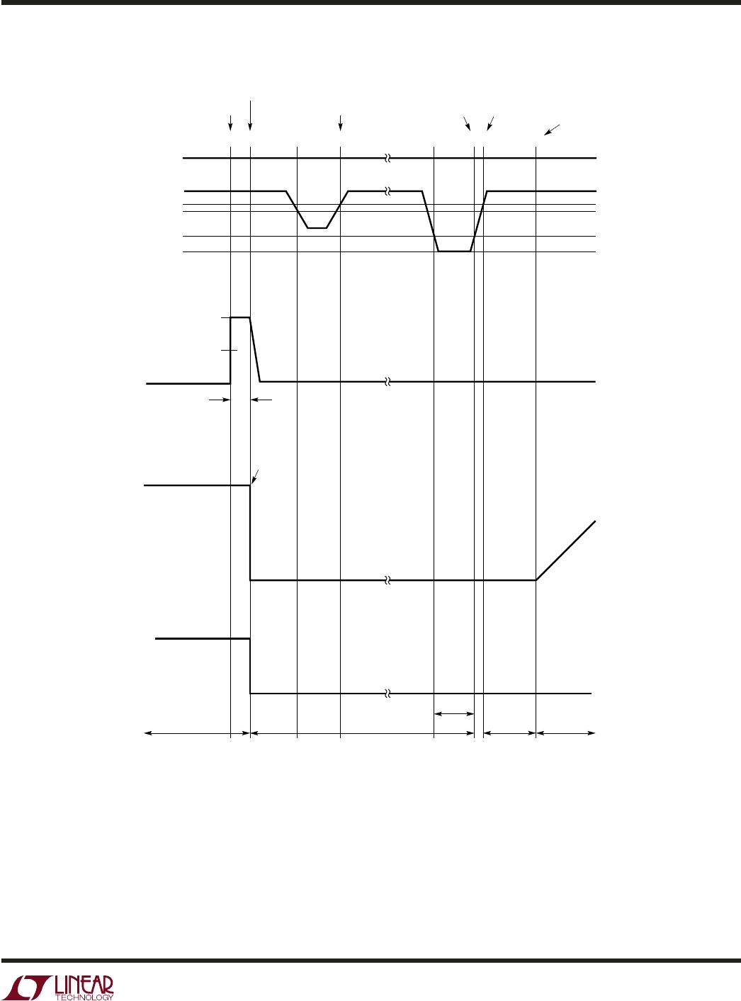
Load Supply Power-Up after Circuit Breaker Armed
Figure 4 shows a normal power-up sequence for the
circuit in Figure 1 where the V
IN
load supply power-up after
circuit breaker is armed. V
CC
is first powered up by an
auxiliary bias supply. V
CC
rises above 2.07V at time
point 1. V
ON
exceeds 0.8V at time point 2. After a 60µs
debounce delay, the GATE pin starts ramping up at time
point 3. The external MOSFET starts conducting at time
point 4. At time point 5, V
GATE
exceed ∆V
GSARM
and the
circuit breaker is armed. After 50µs (t
READY
delay), READY
pulls high by an external resistor at time point 6. READY
signals the V
IN
load supply module to start its ramp. The
load supply begins soft-start ramp at time point 7. The load
supply ramp rate must be slow to prevent circuit breaker
tripping as in equation (8).
∆
∆
V
t
II
C
IN OPMAX LOAD
LOAD
<
−
()8
Where I
OPMAX
is the maximum operating current defined
by equation 7.
For illustration, V
CB
= 25mV and R
DSON
= 3.5mΩ at the
nominal operating ∆V
GSMAX
. The maximum operating
current is 3.5A (refer to equation 7). Assuming the load
can draw a current of 2A at power-up, there is a margin of
1.5A available for C
LOAD
of 100µF and V
IN
ramp rate should
be <15V/ms. At time point 8, the current through the
MOSFET reduces after C
LOAD
is fully charged.
APPLICATIO S I FOR ATIO
WUU
U