LTC4213
16
4213f
APPLICATIO S I FOR ATIO
WUU
U
Figure 5. Load Supply Power-Up Before V
CC
V
ON
> 0.8V
V
th
01 2 3 4 56 7 8
V
CC
, V
ON
CIRCUIT BREAKER ARMS
READY SIGNALS
V
READY
V
SENSEN
V
SENSEP
RESET MODE NORMAL CYCLE
t
READY
STARTUP CYCLE
t
DEBOUNCE
V
GATE
4213 F05
V
SENSEP
– V
SENSEN
= V
CB
V
GATE
MAXES OUT
V
CC
> 2.07V
V
GSARM
+ V
SENSEN
V
GSMAX
+ V
SENSEN
Load Supply Power-Up Before V
CC
Referring back to Figure 1, the V
IN
load supply can also be
powered up before V
CC
. Figure 5 shows the timing dia-
gram with the V
IN
load supply active initially. An internal
circuit ensures that the GATE pin is held low. At time point
1, V
CC
clears UVLO and at time point 2, ON clears 0.8V.
60µs later at time point 3, the GATE is ramped up with
100µA. At time point 4, GATE reaches the external MOSFET
threshold V
TH
and V
OUT
starts to ramp up. At time point 5,
V
SENSEN
is near its peak. At time point 6, the circuit breaker
is armed and the circuit breaker can trip if V
SENSE
> V
CB
.
At time point 7, the GATE voltage peaks. 50µs after time
point 6, READY goes HIGH.
Startup Problems
There is no current limit monitoring during output charg-
ing for the figure 5 power-up sequence where the load
supply is powered up before V
CC
. This is because the GATE
voltage is below V
GSARM
and the MOSFET may not reach
the specified R
DSON
. The V
IN
load supply should have
sufficient capability to handle the inrush as the output
charges up. For proper startup, the final load at time
LTC4213
17
4213f
The selected MOSFET V
GS
absolute maximum rating should
meet the LTC4213 maximum V
GSMAX
of 8V.
Other MOSFET criteria such as V
BDSS
, I
DMAX
, and R
DSON
should be reviewed. Spikes and ringing above maximum
operating voltage should be considered when choosing
V
BDSS
. I
DMAX
should be greater than the current limit. The
maximum operating load current is determined by the
R
DSON
value. See the section on “Calculating Current
Limit” for details.
Supply Requirements
The LTC4213 can be powered from a single supply or dual
supply system. The load supply is connected to the
SENSEP pin and the drain of the external MOSFET. In the
single supply case, the V
CC
pin is connected to the load
supply, preferably with an RC filter. With dual supplies,
V
CC
is connected to an auxiliary bias supply V
AUX
where
V
AUX
voltage should be greater or equal to the load supply
voltage. The load supply voltage must be capable of
sourcing more current than the circuit breaker limit. If the
load supply current limit is below the circuit breaker trip
current, the LTC4213 may not react when the output
overloads. Furthermore, output overloads may trigger
UVLO if the load supply has foldback current limit in a
single supply system.
V
IN
Transient and Overvoltage Protection
Input transient spikes are commonly observed whenever
the LTC4213 responds to overload. These spikes can be
large in amplitude, especially given that large decoupling
capacitors are absent in hot swap environments. These
short spikes can be clipped with a transient suppressor of
adequate voltage and power rating. In addition, the LTC4213
can detect a prolonged overvoltage condition. When
APPLICATIO S I FOR ATIO
WUU
U
point 6 should be within the circuit breaker limits. Other-
wise, the system fails to start and the circuit breaker trips
immediately after arming. In most applications additional
external gate capacitance is not required unless C
LOAD
is
large and startup becomes problematic. If an external gate
capacitor is employed, its capacitance value should not be
excessive unless it is used with a series resistor. This is
because a big gate capacitor without resistor slows down
the GATE turn off during a fault. An alternative method
would be a stepped I
SEL
pin to allow a higher current limit
during startup.
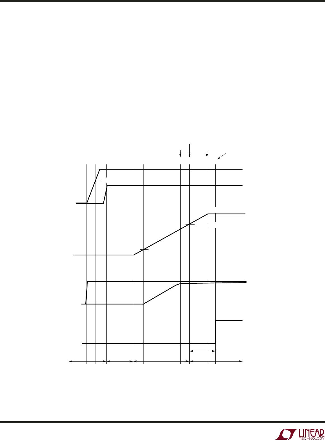
In the event of output short circuit or a severe overload, the
load supply can collapse during GATE ramp up due to load
supply current limit. The chosen MOSFET must withstand
this possible brief short circuit condition before time
point 6 where the circuit breaker is allowed to trip. Bench
short circuit evaluation is a practical verification of a
reliable design. To have current limit while powering a
MOSFET into short circuit conditions, it is preferred that
the load supply sequences to turn on after the circuit
breaker is armed as described in an earlier section.
Power-Off Cycle
The system can be powered off by toggling the ON pin low.
When ON is brought below 0.76V for 5µs, the GATE and
READY pins are pulled low. The system resets when ON is
brought below 0.4V for 80µs.
MOSFET Selection
The LTC4213 is designed to be used with logic (5V) and
sub-logic (3V) MOSFETs for V
CC
potentials above 2.97V
with V
GSMAX
exceeding 4.5V. For a V
CC
supply range
between 2.3V and 2.97V, sub-logic MOSFETs should be
used as the minimum V
GSMAX
is less than 4.5V.
LTC4213
18
4213f
APPLICATIO S I FOR ATIO
WUU
U
4213 F06
+
LTC4213
V
CC
ON READY
C1
10µF
C
LOAD
100µF
R4
10k
I
SEL
GND
GATE
Q1
SI4410DY
Q2
2N7002
V
IN
V
OUT
5V
1A
SENSENSENSEP
C
IN
100µF
R1
33
D1
MBRO520L
R3
324k
R2
80.6k
RESET
V
IN
5V
+
C2
0.22µF
Figure 6. Single Supply Electronic Fuse
SENSEP exceeds V
CC
+ 0.7V for more than 65µs, the
LTC4213’s internal overvoltage protection circuit acti-
vates and the GATE pin pulls down and turns off the
external MOSFET.
Typical Electronic Fuse Application for a Single
Supply System
Figure 6 shows a single supply electronic fuse application.
An RC filter at V
CC
pin filters out transient spikes. An
optional Schottky diode can be added if severe V
CC
dips
during a fault start-up condition is a concern. The use of
the Schottky and RC filter combination is allowed if the
load supply is above 2.9V and the total voltage drop
towards the V
CC
pin is less than 0.4V. The LTC4213’s
internal UVLO filter further rejects bias supply’s transients
of less than t
RESET
. During power-up, it is good engineer-
ing practice to ensure that V
CC
is fully established before
the ON pin enables the system at V
ON
= 0.8V. In this
application, the V
CC
voltage reached final value approxi-
mately after a 5.3 • R
1
C
1
delay. This is followed by the ON
pin exceeding 0.8V after a 0.17 • R
2
C
2
delay. The GATE pin
starts up after an internal t
DEBOUNCE
delay.
Hot Swap is a trademark of Linear Technology Corporation.
Typical Single Supply Hot Swap™ Application
A typical single supply Hot Swap application is shown in
Figure 7. The RESET signal at the backplane is held low
initially. When the PCB long edge makes contact the ON
pin is held low (<0.4V) and the LTC4213 is kept in reset
mode. When the short edge makes contact the V
IN
load
supply is connected to the card. The V
CC
is biased via the
RC filter. The V
OUT
is pre-charged via R5. To power-up
successfully, the R5 resistor value should be small enough
to provide the load requirement and to overcome the
280µA current source sinking into the SENSEN pin. On the
other hand, the R5 resistor value should be big enough
avoiding big inrush current and preventing big short
circuit current. When RESET signals high at backplane, C2
capacitor at the ON pin charges up via the R3/R2 resistive
divider. When ON pin voltage exceeds 0.8V, the GATE pin
begins to ramp up. When the GATE voltage peaks, the
external MOSFET is fully turned on and the V
IN
-to-V
OUT
voltage drop reduces. In normal mode operation, the
LTC4213 monitors the load current through the R
DSON
of
the external MOSFET.

LTC4213CDDB#TRPBF

Mfr. #:
Manufacturer:
Analog Devices Inc.
Description:
Hot Swap Voltage Controllers No RSENSE Electronic Circ Breaker
Lifecycle:
New from this manufacturer.
Delivery:
DHL FedEx Ups TNT EMS
Payment:
T/T Paypal Visa MoneyGram Western Union