6.42
IDT7133SA/LA, IDT7143SA/LA
High-Speed 2K x 16 Dual-Port RAM Military, Industrial and Commercial Temperature Ranges
2
2746 drw 02
10
11
12
13
14
15
16
IDT7133/43
J68-1 / F68-1
(4)
68-Pin PLCC/Flatpack
Top View
(5)
50
49
48
47
46
45
44
INDEX
17
18
19
20
21
22
23
24
25
26
51
52
53
54
55
56
57
58
59
60
987 6543 2
1
68 67 66 65 64 63 62 61
27 28 29 30 31 32 33 34 35 36 37 38 39 40 41 42 43
A
6L
A
5L
A
4L
A
3L
A
2L
A
1L
A
0L
A
0R
A
1R
A
2R
A
3R
A
4R
A
5R
BUSY
L
BUSY
R
CE
L
CE
R
I/O
9L
I/O
10L
I/O
11L
I/O
13L
I/O
14L
I/O
15L
V
CC
(1)
I/O
0R
I/O
1R
I/O
2R
I/O
3R
I/O
4R
I/O
5R
I/O
6R
I/O
7R
I
/
O
1
L
I
/
O
2
L
I
/
O
3
L
I
/
O
4
L
I
/
O
5
L
I
/
O
6
L
I
/
O
7
L
I
/
O
8
L
V
C
C
(
1
)
A
1
0
L
A
9
L
A
8
L
A
7
L
R
/
W
L
L
B
O
E
L
I
/
O
9
R
I
/
O
1
0
R
I
/
O
1
2
R
I
/
O
1
3
R
I
/
O
1
4
R
I
/
O
1
5
R
A
6
R
A
7
R
A
8
R
A
9
R
I
/
O
8
R
A
1
0
R
G
N
D
(
2
)
O
E
R
R
/
W
R
L
B
R
/
W
R
U
B
I
/
O
1
1
R
I
/
O
0
L
I/O
12L
GND
(2)
R
/
W
L
U
B
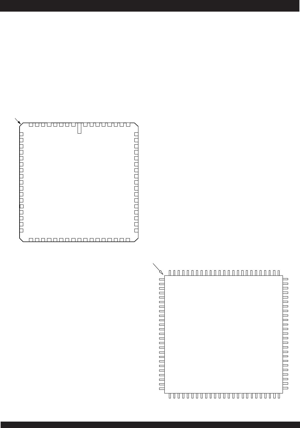
Pin Configurations
(1,2,3)
Description
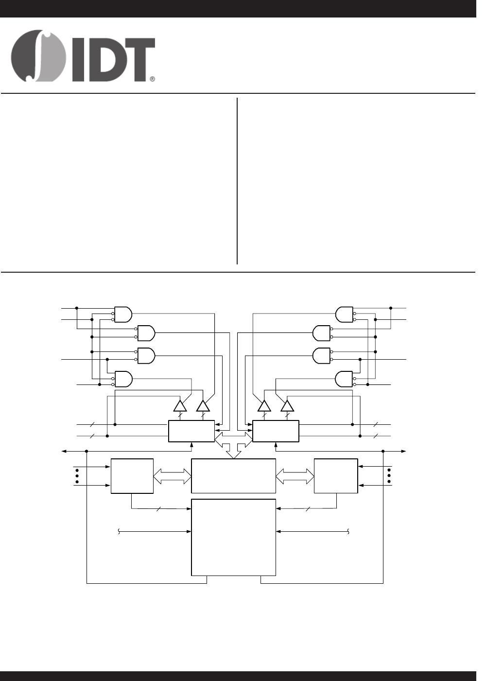
The IDT7133/7143 are high-speed 2K x 16 Dual-Port Static RAMs.
The IDT7133 is designed to be used as a stand-alone 16-bit Dual-Port
RAM or as a “MASTER” Dual-Port RAM together with the IDT7143
“SLAVE” Dual-Port in 32-bit-or-more word width systems. Using the IDT
MASTER/SLAVE Dual-Port RAM approach in 32-bit-or-wider memory
system applications results in full-speed, error-free operation without the
need for additional discrete logic.
Both devices provide two independent ports with separate control,
address, and I/O pins that permit independent, asynchronous access for
reads or writes to any location in memory. An automatic power down
feature, controlled by CE, permits the on-chip circuitry of each port to enter
a very low standby power mode.
Fabricated using CMOS high-performance technology. Low-power
(LA) versions offer battery backup data retention capability, with each port
typically consuming 200µW for a 2V battery.
The IDT7133/7143 devices have identical pinouts. Each is packed in
a 68-pin ceramic PGA, 68-pin flatpack, 68-pin PLCC and 100-pin TQFP.
Military grade product is manufactured in compliance with the latest revision
of MIL-PRF-38535 QML, making it ideally suited to military temperature
applications demanding the highest level of performance and reliability.
NOTES:
1. Both V
CC pins must be connected to the power supply to ensure reliable
operation.
2. Both GND pins must be connected to the ground supply to ensure reliable
operation.
3. J68-Package body is approximately 0.95 in x 0.95 in x 0.17 in.
F68-Package body is approximately 1.18 in x 1.18 in x 0.16 in.
PN100-Package body is approximately 14mm x 14mm x 1.4mm.
4. This package code is used to reference the package diagram.
5. This text does not indicate orientation of the actual part-marking.
Index
1
2
3
4
5
6
7
8
9
10
11
12
13
14
15
16
17
18
19
20
21
22
23
24
25
75
74
73
72
71
70
69
68
67
66
65
64
63
62
61
60
59
58
57
56
55
54
53
52
51
26 27 28 29 30 31 32 33 34 35 36 37 38 39 40 41 42 43 44 45 46 47 48 49 50
100999897969594939291908988878685848382818079787776
IDT7133/43PF
PN100-1
(4)
100-Pin TQFP
Top View
(5)
N/C
N/C
N/C
N/C
I/O
10L
I/O
11L
I/O
12L
I/O
13L
GND
I/O
14L
I/O
15L
V
CC
GND
I/O
0R
I/O
1R
I/O
2R
I/O
3R
V
CC
I/O
4R
I/O
5R
I/O
6R
N/C
N/C
N/C
N/C
274 6 drw 03
N/C
N/C
N/C
N/C
A
5L
A
4L
A
3L
A
2L
A
1L
A
0L
N/C
GND
N/C
BUSY
R
N/C
A
0R
N/C
N/C
N/C
N/C
BUSY
L
A
1R
A
2R
A
3R
A
4R
I
/
O
9
L
I
/
O
8
L
I
/
O
7
L
I
/
O
6
L
I
/
O
5
L
I
/
O
4
L
I
/
O
3
L
I
/
O
2
L
G
N
D
I
/
O
1
L
I
/
O
0
L
O
E
L
V
C
C
R
/
W
L
L
B
C
E
L
R
/
W
L
U
B
N
/
C
N
/
C
N
/
C
A
1
0
L
A
9
L
A
8
L
A
7
L
A
6
L
I
/
O
7
R
I
/
O
8
R
I
/
O
9
R
I
/
O
1
0
R
I
/
O
1
1
R
I
/
O
1
2
R
I
/
O
1
3
R
I
/
O
1
4
R
G
N
D
I
/
O
1
5
R
R
/
W
R
L
B
G
N
D
N
/
C
N
/
C
A
1
0
R
A
9
R
A
8
R
A
7
R
A
6
R
A
5
R
N
/
C
N
/
C
N
/
C
O
E
R
C
E
R
R
/
W
R
U
B