6.42
IDT7133SA/LA, IDT7143SA/LA
High-Speed 2K x 16 Dual-Port RAM Military, Industrial and Commercial Temperature Ranges
7
AC Electrical Characteristics Over the
Operating Temperature and Supply Voltage
(3)
NOTES:
1. Transition is measured 0mV fromLow or High-impedance voltage with load (Figure 2).
2. This parameter is guaranteed by device characterization, but is not production tested.
3. 'X' in part number indicates power rating (SA or LA).
7133X20
7143X20
Com'l Only
7133X25
7143X25
Com'l & Ind
7133X35
7143X35
Com'l
& Military
UnitSymbol Parameter Min.Max.Min.Max.Min.Max.
READ CYCLE
t
RC
Read Cycle Time 20
____
25
____
35
____
ns
t
AA
Address Access Time
____
20
____
25
____
35 ns
t
ACE
Chip Enable Access Time
____
20
____
25
____
35 ns
t
AOE
Output Enable Access Time
____
12
____
15
____
20 ns
t
OH
Output Hold from Address Change 0
____
0
____
0
____
ns
t
LZ
Output Low-Z Time
(1,2)
0
____
0
____
0
____
ns
t
HZ
Output High-Z Time
(1,2)
____
12
____
15
____
20 ns
t
PU
Chip Enable to Power Up Time
(2)
0
____
0
____
0
____
ns
t
PD
Chip Disable to Power Down Time
(2)
____
20
____
50
____
50 ns
2746 tbl 10a
7133X45
7143X45
Com'l Only
7133X55
7143X55
Com'l, Ind
& Military
7133X70/90
7143X70/90
Com'l &
Military
UnitSymbol Parameter Min.Max.Min.Max.Min.Max.
READ CYCLE
t
RC
Read Cycle Time 45
____
55
____
70/90
____
ns
t
AA
Address Access Time
____
45
____
55
____
70/90 ns
t
ACE
Chip Enable Access Time
____
45
____
55
____
70/90 ns
t
AOE
Output Enable Access Time
____
25
____
30
____
40/40 ns
t
OH
Output Hold from Address Change 0
____
0
____
0/0
____
ns
t
LZ
Output Low-Z Time
(1,2)
0
____
5
____
5/5
____
ns
t
HZ
Output High-Z Time
(1,2)
____
20
____
20
____
25/25 ns
t
PU
Chip Enable to Power Up Time
(2)
0
____
0
____
0/0
____
ns
t
PD
Chip Disable to Power Down Time
(2)
____
50
____
50
____
50/50 ns
2746 tbl 10b
6.42
IDT7133SA/LA, IDT7143SA/LA
High-Speed 2K x 16 Dual-Port RAM Military, Industrial and Commercial Temperature Ranges
8
TIMING WAVEFORM OF READ CYCLE NO. 1, EITHER SIDE
(5)
TIMING WAVEFORM OF READ CYCLE NO. 2, EITHER SIDE
(5)
NOTES:
1. Timing depends on which signal is asserted last, OE or CE.
2. Timing depends on which signal is deasserted first, OE or CE.
3. t
BDD delay is required only in a case where the opposite port is completing a write operation to the same address location. For simultaneous read operations, BUSY has no
relationship to valid output data.
4. Start of valid data depends on which timing becomes effective last, t
AOE, tACE, tAA, or tBDD.
5. R/W = V
IH, and the address is valid prior to or coincidental with CE transition LOW.
2746 drw 07
t
AA
t
OH
t
OH
DATA
OUT
ADDRESS
t
RC
DATA VALIDPREVIOUS DATA VALID
BUSY
OUT
t
BDD
(3,4)
2746 drw 08
t
AOE
t
LZ
t
HZ
DATA
OUT
CE
t
ACE
VALID DATA
OE
CURRENT
I
CC
I
SB
t
PU
50%
t
LZ
t
PD
50%
t
HZ
(1)
(4)
(1)
(4)
(2)
(2)
6.42
IDT7133SA/LA, IDT7143SA/LA
High-Speed 2K x 16 Dual-Port RAM Military, Industrial and Commercial Temperature Ranges
9
AC Electrical Characteristics Over the
Operating Temperature and Supply Voltage
(5)
NOTES:
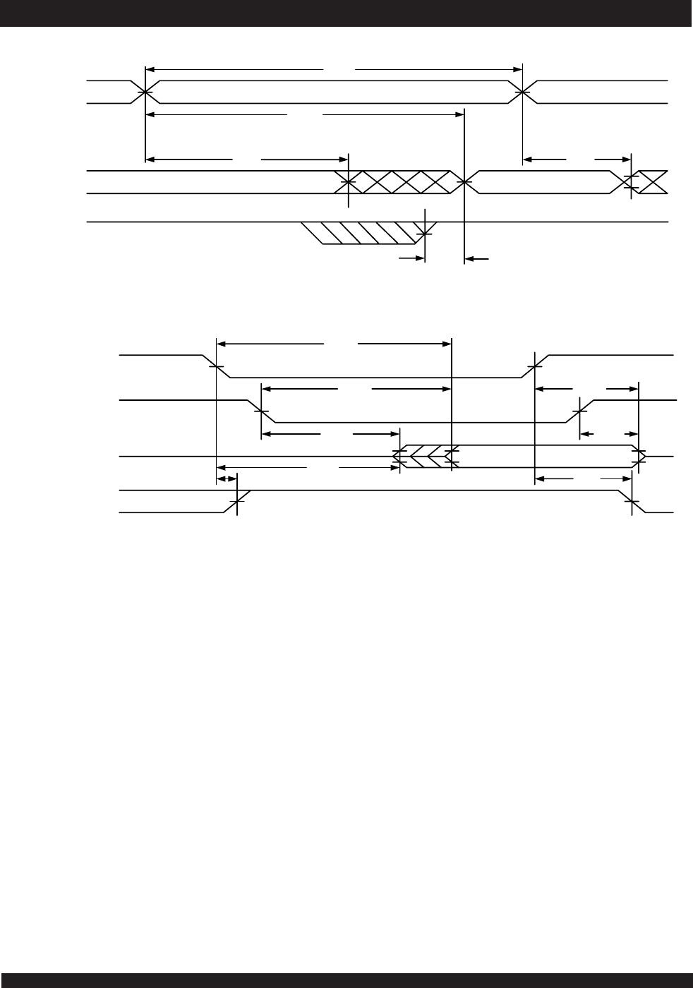
1. Transition is measured 0mV from Low or High-impedance voltage from the Output Test Load (Figure 2).
2. This parameter is guaranteed by device characterization but not production tested.
3. For MASTER/SLAVE combination, t
WC = tBAA + tWR + tWP, since R/W = VIL must occur after tBAA.
4. The specification for tDH must be met by the device supplying write data to the RAM under all operation conditions. Although tDH and tOW values will vary over voltage
and temperature, the actual t
DH will always be smaller than the actual tOW.
5. 'X' in part number indicates power rating (SA or LA).
Symbol Parameter
7133X45
7143X45
Com'l Only
7133X55
7143X55
Com'l, Ind
& Military
7133X70/90
7143X70/90
Com'l &
Military
UnitMin. Max. Min. Max. Min. Max.
WRITE CYCLE
t
WC
Write Cycle Time
(3)
45
____
55
____
70/90
____
ns
t
EW
Chip Enable to End-of-Write 30
____
40
____
50/50
____
ns
t
AW
Address Valid to End-of-Write 30
____
40
____
50/50
____
ns
t
AS
Address Set-up Time 0
____
0
____
0/0
____
ns
t
WP
Write Pulse Width 30
____
40
____
50/50
____
ns
t
WR
Write Recovery Time 0
____
0
____
0/0
____
ns
t
DW
Data Valid to End-of-Write 20
____
25
____
30/30
____
ns
t
HZ
Output High-Z Time
(1,2)
____
20
____
20
____
25/25 ns
t
DH
Data Ho ld Time
(4)
5
____
5
____
5/5
____
ns
t
WZ
Write Enable to Output in High-Z
(1,2)
____
20
____
20
____
25/25 ns
t
OW
Outp ut Active from End -o f-Write
(1,2,4)
5
____
5
____
5/5
____
ns
2746 tbl 11b
Symbol Parameter
7133X20
7143X20
Com'l Only
7133X25
7143X25
Com'l & Ind
7133X35
7143X35
Com'l
& Military
UnitMin. Max. Min. Max. Min. Max.
WRITE CYCLE
t
WC
Write Cycle Time
(3)
20
____
25
____
35
____
ns
t
EW
Chip Enable to End-of-Write 15
____
20
____
25
____
ns
t
AW
Address Valid to End-of-Write 15
____
20
____
25
____
ns
t
AS
Address Set-up Time 0
____
0
____
0
____
ns
t
WP
Write Pulse Width 15
____
20
____
25
____
ns
t
WR
Write Recovery Time 0
____
0
____
0
____
ns
t
DW
Data Valid to End-of-Write 15
____
15
____
20
____
ns
t
HZ
Output High-Z Time
(1,2)
____
12
____
15
____
20 ns
t
DH
Data Hold Time
(4)
0
____
0
____
0
____
ns
t
WZ
Write Enable to Output in High-Z
(1,2)
____
12
____
15
____
20 ns
t
OW
Output Active from End-of-Write
(1,2,4)
0
____
0
____
0
____
ns
2746 tb l 11a

7133LA45J

Mfr. #:
Manufacturer:
IDT
Description:
SRAM 32K(2KX16)CMOS DUALPORT R
Lifecycle:
New from this manufacturer.
Delivery:
DHL FedEx Ups TNT EMS
Payment:
T/T Paypal Visa MoneyGram Western Union