6.42
IDT7133SA/LA, IDT7143SA/LA
High-Speed 2K x 16 Dual-Port RAM Military, Industrial and Commercial Temperature Ranges
14
Functional Description
The IDT7133/43 provides two ports with separate control, address
and I/O pins that permit independent access for reads or writes to any
location in memory. The IDT7133/43 has an automatic power down
feature controlled by CE. The CE controls on-chip power down circuitry
that permits the respective port to go into a standby mode when not
selected (CE HIGH). When a port is enabled, access to the entire
memory array is permitted. Non-contention READ/WRITE conditions
are illustrated in Truth Table 1.
Busy Logic
Busy Logic provides a hardware indication that both ports of the
RAM have accessed the same location at the same time. It also allows
one of the two accesses to proceed and signals the other side that the
RAM is “busy”. The BUSY pin can then be used to stall the access until
the operation on the other side is completed. If a write operation has
been attempted from the side that receives a BUSY indication, the
write signal is gated internally to prevent the write from proceeding.
The use of BUSY logic is not required or desirable for all applica-
tions. In some cases it may be useful to logically OR the BUSY outputs
together and use any BUSY indication as an interrupt source to flag the
event of an illegal or illogical operation. If the write inhibit function of
BUSY logic is not desirable, the BUSY logic can be disabled by using
the IDT7143 (SLAVE). In the IDT7143, the BUSY pin operates solely
as a write inhibit input pin. Normal operation can be programmed by
tying the BUSY pins HIGH. If desired, unintended write operations can
be prevented to a port by tying the BUSY pin for that port LOW. The
BUSY outputs on the IDT 7133 RAM are open drain and require pull-
up resistors.
Width Expansion with Busy Logic
Master/Slave Arrays
When expanding an IDT7133/43 RAM array in width while using
BUSY logic, one master part is used to decide which side of the RAM
array will receive a BUSY indication, and to output that indication. Any
number of slaves to be addressed in the same address range as the
master, use the BUSY signal as a write inhibit signal. Thus on the
IDT7133 RAM the BUSY pin is an output and on the IDT7143 RAM, the
BUSY pin is an input (see Figure 3).
Expanding the data bus width to 32 bits or more in a Dual-Port RAM
system implies that several chips will be active at the same time. If each
chip includes a hardware arbitrator, and the addresses for each chip
arrive at the same time, it is possible that one will activate its BUSY
L
while another activates its BUSYR signal. Both sides are now BUSY
and the CPUs will await indefinitely for their port to become free.
To avoid the “Busy Lock-Out” problem, IDT has developed a
MASTER/SLAVE approach where only one hardware arbitrator, in the
MASTER, is used. The SLAVE has BUSY inputs which allow an
interface to the MASTER with no external components and with a
speed advantage over other systems.
When expanding Dual-Port RAMs in width, the writing of the SLAVE
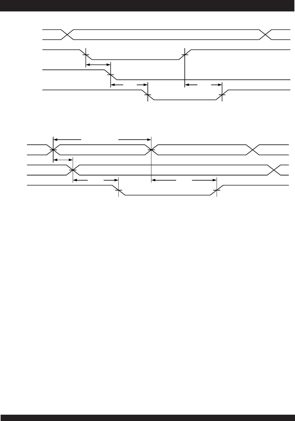
RAMs must be delayed until after the BUSY input has settled.
Otherwise, the SLAVE chip may begin a write cycle during a contention
situation. Conversely, the write pulse must extend a hold time past
BUSY to ensure that a write cycle takes place after the contention is
resolved. This timing is inherent in all Dual-Port memory systems where
more than one chip is active at the same time.
The write pulse to the SLAVE should be delayed by the maximum
arbitration time of the MASTER. If, then, a contention occurs, the write
to the SLAVE will be inhibited due to BUSY from the MASTER.
Figure 4. Busy and chip enable routing for both width and depth expansion
with the IDT7133 (MASTER) and the IDT7143 (SLAVE).
V
CC
R/W
BUSY
R/W
BUSY
IDT7133
MASTER
V
CC
R/W
BUSY
R/W
BUSY
R/W
BUSY
R/W
BUSY
LEFT
RIGHT
2746 drw 15
IDT7143
SLAVE
270Ω
270Ω