TC642
DS21444D-page 10 2001-2012 Microchip Technology Inc.
FIGURE 5-2: Temperature Sensing
Circuit.
Generally, the thermistor shown in Figure 5-2 is a non-
linear device with a negative temperature coefficient
(also called an NTC thermistor). In Figure 5-2, R
1
is
used to linearize the thermistor temperature response,
while R
2
is used to produce a positive temperature
coefficient at the V
IN
node. As an added benefit, this
configuration produces an output voltage delta of 1.4V,
which is well within the range of the V
C(SPAN)
specification of the TC642. A 100 kNTC thermistor is
selected for this application in order to keep I
DIV
at a
minimum.
For the voltage range at V
IN
to be equal to 1.25V to
2.65V, the temperature range of this configuration is
0°C to 50°C. If a different temperature range is required
from this circuit, R
1
should be chosen to equal the
resistance value of the thermistor at the center of this
new temperature range. With this change, R
2
is
adjusted according to the formulas below. It is
suggested that a maximum temperature range of 50°C
be used with this circuit due to thermistor linearity
limitations.
The following two equations permit solving for the two
unknown variables, R
1
and R
2
. More information
regarding thermistors can be found in AN679, “Temper-
ature Sensing Technologies”, and AN685, “Thermistors
in Single Supply Temperature Sensing Circuits”, which
can be downloaded from Microchip’s web site at:
www.microchip.com.
EQUATION
5.2 Minimum Fan Speed
A voltage divider on V
MIN
sets the minimum PWM duty
cycle and, thus, the minimum fan speed. As with the
V
IN
input, 1.25V to 2.65V typically corresponds to 0%
to 100% duty cycle. Assuming that fan speed is linearly
related to duty cycle, the minimum speed voltage is
given by the equation:
EQUATION
For example, if 2500 RPM equates to 100% fan speed,
and a minimum speed of 1000 RPM is desired, then
the V
MIN
voltage is:
EQUATION
The V
MIN
voltage may be set using a simple resistor
divider, as shown in Figure 5-3. Per Section 1.0,
“Electrical Characteristics”, the leakage current at the
V
MIN
pin is no more than 1 µA. It would be very
conservative to design for a divider current, I
DIV
, of
100 µA. If V
DD
= 5.0V then;
EQUATION
FIGURE 5-3: V
IN
Circuit.
R
2
= 23.2 kΩ
R
1
= 100 kΩ
NTC Thermistor
100 kΩ @ 25˚C
RT
1
I
DIV
V
IN
V
DD
V
DD
x R
2
R
TEMP
(T
1
) + R
2
= V(T
1
)
R
TEMP
(T
2
) + R
2
= V(T
2
)
V
DD
x R
2
Where T
1
and T
2
are the chosen temperatures and
R
TEMP
is the parallel combination of the thermistor
and R
1
.
Minimum Speed
Full Speed
V
MIN
=
x (1.4) + 1.25V
1000
2500
V
MIN
=
x (1.4) + 1.25V = 1.81V
R
1
+ R
2
I
DIV
= 100µA = , therefore
5.0V
R
1
+ R
2
= = 50,000 = 50k
100µA
5.0V
2001-2012 Microchip Technology Inc. DS21444D-page 11
TC642
We can further specify R
1
and R
2
by the condition that
the divider voltage is equal to our desired V
MIN
. This
yields the following equation:
EQUATION
Solving for the relationship between R
1
and R
2
results
in the following equation:
EQUATION
In this example, R
1
= (1.762) R
2
. Substituting this rela-
tionship back into the previous equation yields the
resistor values:
R
2
= 18.1 k, and R
1
= 31.9 k
In this case, the standard values of 31.6 k and
18.2 k are very close to the calculated values and
would be more than adequate.
5.3 Operations at Low Duty Cycle
One boundary condition which may impact the selec-
tion of the minimum fan speed is the irregular activation
of the Diagnostic Timer due to the TC642 “missing” fan
commutation pulses at low speeds. This is a natural
consequence of low PWM duty cycles (typically 25% or
less). Recall that the SENSE function detects commu-
tation of the fan as disturbances in the current through
R
SENSE
. These can only occur when the fan is ener-
gized (i.e., V
OUT
is “on”). At very low duty cycles, the
V
OUT
output is “off” most of the time. The fan may be
rotating normally, but the commutation events are
occurring during the PWM’s off-time.
The phase relationship between the fan’s commutation
and the PWM edges tends to “walk around” as the
system operates. At certain points, the TC642 may fail
to capture a pulse within the 32-cycle missing pulse
detector window. When this happens, the 3-cycle
Diagnostic Timer will be activated, the V
OUT
output will
be active continuously for three cycles and, if the fan is
operating normally, a pulse will be detected. If all is
well, the system will return to normal operation. There
is no harm in this behavior, but it may be audible to the
user as the fan accelerates briefly when the Diagnostic
Timer fires. For this reason, it is recommended that
V
MIN
be set no lower than 1.8V.
5.4 FanSense Network
(R
SENSE
and C
SENSE
)
The FanSense network, comprised of R
SENSE
and
C
SENSE
, allows the TC642 to detect commutation of
the fan motor (FanSense technology). This network
can be thought of as a differentiator and threshold
detector. The function of R
SENSE
is to convert the fan
current into a voltage. C
SENSE
serves to AC-couple this
voltage signal and provide a ground-referenced input to
the SENSE pin. Designing a proper SENSE network is
simply a matter of scaling R
SENSE
to provide the nec-
essary amount of gain (i.e., the current-to-voltage con-
version ratio). A 0.1 µF ceramic capacitor is
recommended for C
SENSE
. Smaller values require
larger sense resistors, and higher value capacitors are
bulkier and more expensive. Using a 0.1 µF capacitor
results in reasonable values for R
SENSE
. Figure 5-4
illustrates a typical SENSE network. Figure 5-5 shows
the waveforms observed using a typical SENSE net-
work.
FIGURE 5-4: SENSE Network.
FIGURE 5-5: SENSE Waveforms.
V
DD
x R
2
R
1
+ R
2
V
MIN
=
V
DD
- V
MIN
V
MIN
R
1
= R
2
x
Q
1
GND
V
DD
R
SENSE
SENSE
R
BASE
C
SENSE
(0.1 μF Typ.)
V
OUT
Fan
1
Ch1
100mV
Tek Run: 10.0kS/s Sample
Ch2 100mV
M5.00ms
Ch1
142mV
GND
[ T ]
T
Waveform @ Sense Resistor
90mV
50mV
GND
Waveform @ Sense Pin
2
TC642
DS21444D-page 12 2001-2012 Microchip Technology Inc.
Table 5-1 lists recommended values for R
SENSE
based
on the nominal operating current of the fan. Note that
the current draw specified by the fan manufacturer may
be a worst-case rating for near-stall conditions and may
not be the fan’s nominal operating current. The values
in Table 5-1 refer to actual average operating current. If
the fan current falls between two of the values listed,
use the higher resistor value. The end result of employ-
ing Table 5-1 is that the signal developed across the
sense resistor is approximately 450 mV in amplitude.
TABLE 5-1: R
SENSE
VS. FAN CURRENT
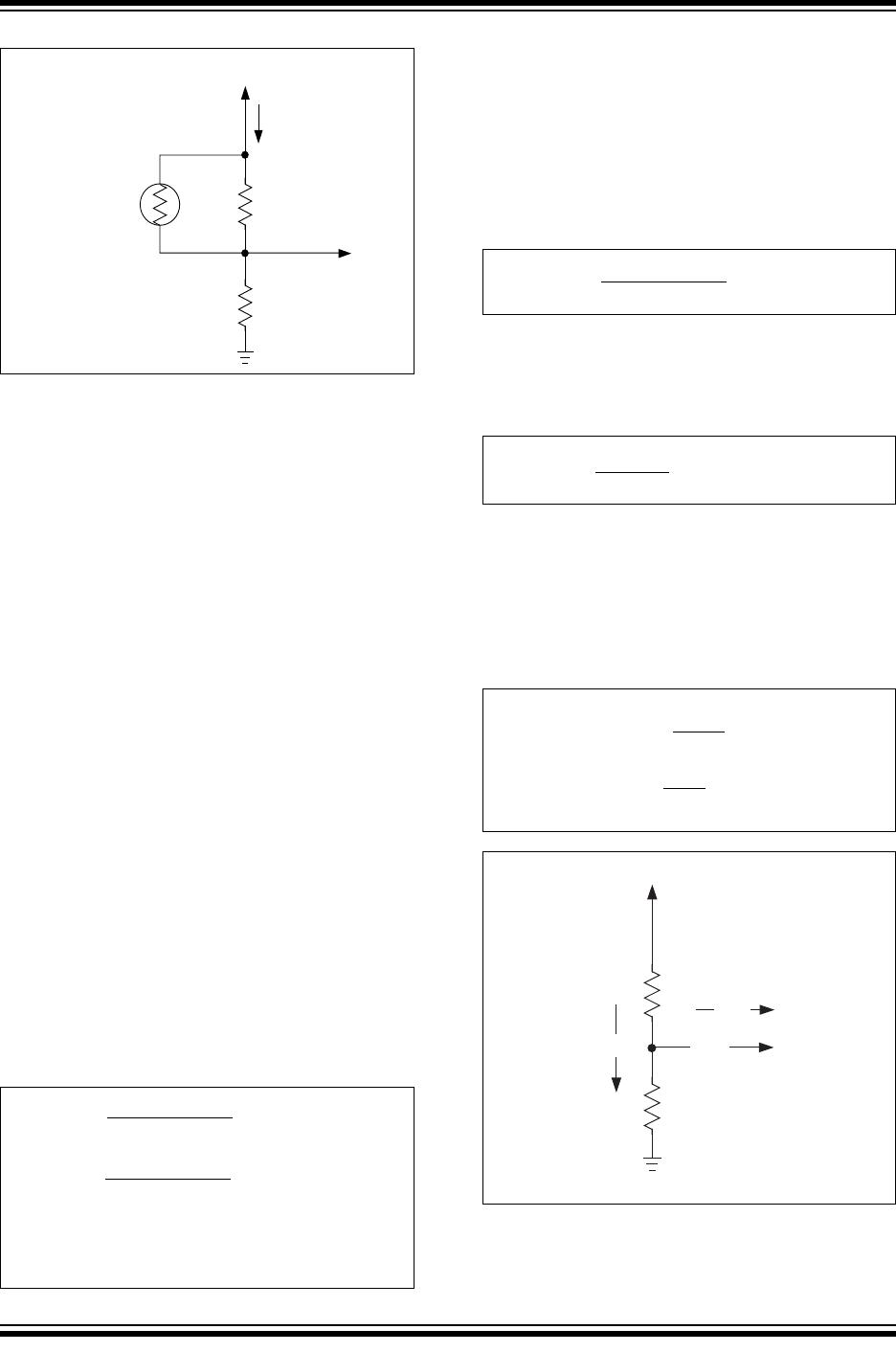
5.5 Output Drive Transistor Selection
The TC642 is designed to drive an external transistor
or MOSFET for modulating power to the fan. This is
shown as Q
1
in Figures 3-1, 5-1, 5-4, 5-6, 5-7, 5-8
and 5-9. The V
OUT
pin has a minimum source current
of 5 mA and a minimum sink current of 1 mA. Bipolar
transistors or MOSFETs may be used as the power
switching element, as shown in Figure 5-7. When high
current gain is needed to drive larger fans, two transis-
tors may be used in a Darlington configuration. Three
possible circuit topologies are shown in Figure 5-7: (a)
shows a single NPN transistor used as the switching
element; (b) illustrates the Darlington pair; and (c)
shows an N-channel MOSFET.
One major advantage of the TC642’s PWM control
scheme versus linear speed control is that the power
dissipation in the pass element is kept very low. Gener-
ally, low cost devices in very small packages, such as
TO-92 or SOT, can be used effectively. For fans with
nominal operating currents of no more than 200 mA, a
single transistor usually suffices. Above 200 mA, the
Darlington or MOSFET solution is recommended. For
the fan sensing function to work correctly, it is impera-
tive that the pass transistor be fully saturated when
“on”.
Table 5-2 gives examples of some commonly available
transistors and MOSFETs. This table should be used
as a guide only since there are many transistors and
MOSFETs which will work just as well as those listed.
The critical issues when choosing a device to use as
Q
1
are: (1) the breakdown voltage (V
(BR)CEO
or V
DS
(MOSFET)) must be large enough to withstand the
highest voltage applied to the fan (Note: This will occur
when the fan is off); (2) 5 mA of base drive current must
be enough to saturate the transistor when conducting
the full fan current (transistor must have sufficient
gain); (3) the V
OUT
voltage must be high enough to suf-
ficiently drive the gate of the MOSFET to minimize the
R
DS(on)
of the device; (4) rated fan current draw must
be within the transistor's/MOSFET's current handling
capability; and (5) power dissipation must be kept
within the limits of the chosen device.
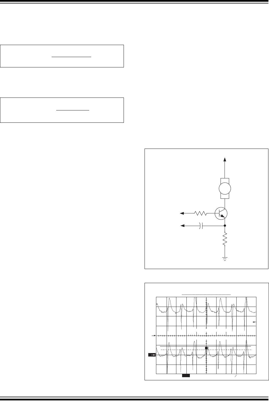
A base-current limiting resistor is required with bipolar
transistors (Figure 5-6).
FIGURE 5-6: Circuit For Determining
R
BASE
.
The correct value for this resistor can be determined as
follows:
V
OH =
V
R
SENSE
+ V
BE
(SAT)
+ V
R
BASE
V
R
SENSE
= I
FAN
x R
SENSE
V
R
BASE
= R
BASE
x I
BASE
I
BASE
= I
FAN
/ h
FE
V
OH
is specified as 80% of V
DD
in Section 1.0, “Electri-
cal Characteristics”; V
BE
(SAT)
is given in the chosen
transistor’s data sheet. It is now possible to solve for
R
BASE
.
EQUATION
Nominal Fan Current (mA) R
SENSE
()
50 9.1
100 4.7
150 3.0
200 2.4
250 2.0
300 1.8
350 1.5
400 1.3
450 1.2
500 1.0
Q
1
GND
V
DD
R
SENS
E
R
BASE
V
OH
= 80% V
DD
+
V
R
BASE
+
V
BE
(SAT)
+
V
R
SENSE
Fan
R
BASE
=
V
OH
- V
BE
(SAT)
- V
R
SENSE
I
BASE

TC642CPA

Mfr. #:
Manufacturer:
Microchip Technology
Description:
Motor / Motion / Ignition Controllers & Drivers w/Fault Dtct
Lifecycle:
New from this manufacturer.
Delivery:
DHL FedEx Ups TNT EMS
Payment:
T/T Paypal Visa MoneyGram Western Union