Sector Subsector Address Range (Byte Addresses in HEX)
Start End
992
3E0000 3E0FFF
1 31
1F000 1FFFF
30
1E000 1EFFF
. . .
18
12000 12FFF
17
11000 11FFF
16
10000 10FFF
0 15
F000 FFFF
14
E000 EFFF
. . .
2
2000 2FFF
1
1000 1FFF
0
H'0000000 H'0000FFF
1.7. Memory Operations
This section describes the operations that you can use to access the memory in EPCQ-
A devices. When performing the operation, addresses and data are shifted in and out
of the device serially, with the MSB first.
1.7.1. Timing Requirements
When the active low chip select (nCS) signal is driven low, shift in the operation code
into the EPCQ-A device using theDATA0 pin. Each operation code bit is latched into the
EPCQ-A device at rising edges of the DCLK signal.
While executing an operation, shift in the desired operation code, followed by the
address or data bytes. See related information for more information about the address
and data bytes. The device must drive the nCS pin high after the last bit of the
operation sequence is shifted in.
For read operations, the data read is shifted out on the DATA[3:0] pins. You can
drive the nCS pin high when any bit of the data is shifted out.
For write and erase operations, drive the nCS pin high at a byte boundary, that is in a
multiple of eight clock pulses. Otherwise, the operation is rejected and not executed.
All attempts to access the memory contents while a write or erase cycle is in progress
are rejected, and the write or erase cycle continues unaffected.
1. EPCQ-A Serial Configuration Device Datasheet
CF52014 | 2018.04.11
EPCQ-A Serial Configuration Device Datasheet
16
1.8. Status Register
Table 16. Status Register Bits
Bit R/W Default
Value
Name Value Description
7 R/W 0
(5)
Reserved
6 R/W 0
(5)
Reserved
5 R/W 0 TB (Top/Bottom
Bit)
1=Protected area starts from the bottom of
the memory array.
0=Protected area starts from the top of the
memory array.
Determine that the
protected area starts
from the top or
bottom of the memory
array.
4 R/W 0 BP2
(6)
Table 17 on page 18 through Table 21 on page
20 list the protected area with reference to
the block protect bits.
Determine the area of
the memory protected
from being written or
erased unintentionally.
3 R/W 0 BP1
(6)
2 R/W 0 BP0
(6)
1 R 0 WEL (Write
Enable Latch
Bit)
1=Allows the following operation to run:
Write Bytes
Write Status Register
Erase Bulk
Erase Sector
0=Rejects the above mentioned operations.
Allows or rejects
certain operation to
run.
0 R 0 WIP (Write in
Progress Bit)
1=One of the following operation is in
progress:
Write Status Register
Write Bytes
Erase
0=no write or erase cycle in progress
Indicates if there is a
command in progress.
1.8.1. Read Status Operation
The status register can be read continuously and at anytime, including during a write
or erase operations.
Figure 4. Read Status Operation Timing Diagram
nCS
DCLK
DATA0
DATA
0 1 2 3 4 5 6 7 8 9 10 11 12 13 14 15
7 6 5 4 3 2 1 0 7 2 1 0 76 5 4 3
Operation Code (05h)
MSB MSB
Status Register Out Status Register Out
High Impedance
(5)
Do not program these bits to 1.
(6)
The erase bulk and erase die operation is only available when all the block protect bits are set
to 0. When any of the block protect bits are set to 1, the relevant area is protected from being
written by a write bytes operation or erased by an erase sector operation.
1. EPCQ-A Serial Configuration Device Datasheet
CF52014 | 2018.04.11
EPCQ-A Serial Configuration Device Datasheet
17
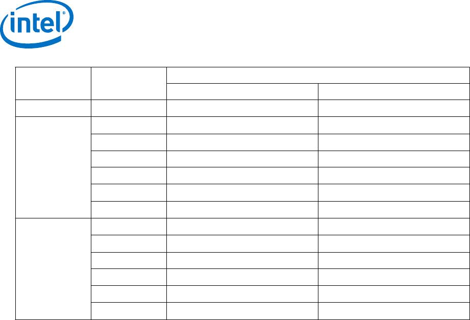
Table 17. Block Protection Bits in EPCQ4A
Status Register Content Memory Content
TB Bit BP2 Bit BP1 Bit BP0 Bit Protected Area Unprotected Area
x 0 0 0 None All sectors
0 0 0 1 Sector 7 Sectors (0 to 6)
0 0 1 0 Sectors (6 to 7) Sectors (0 to 5)
0 0 1 1 Sectors (4 to 7) Sectors (0 to 3)
1 0 0 1 Sector 0 Sectors (1 to 7)
1 0 1 0 Sectors (0 to 1) Sectors (2 to 7)
1 0 1 1 Sectors (0 to 3) Sectors (4 to 7)
x 1 x x All sectors None
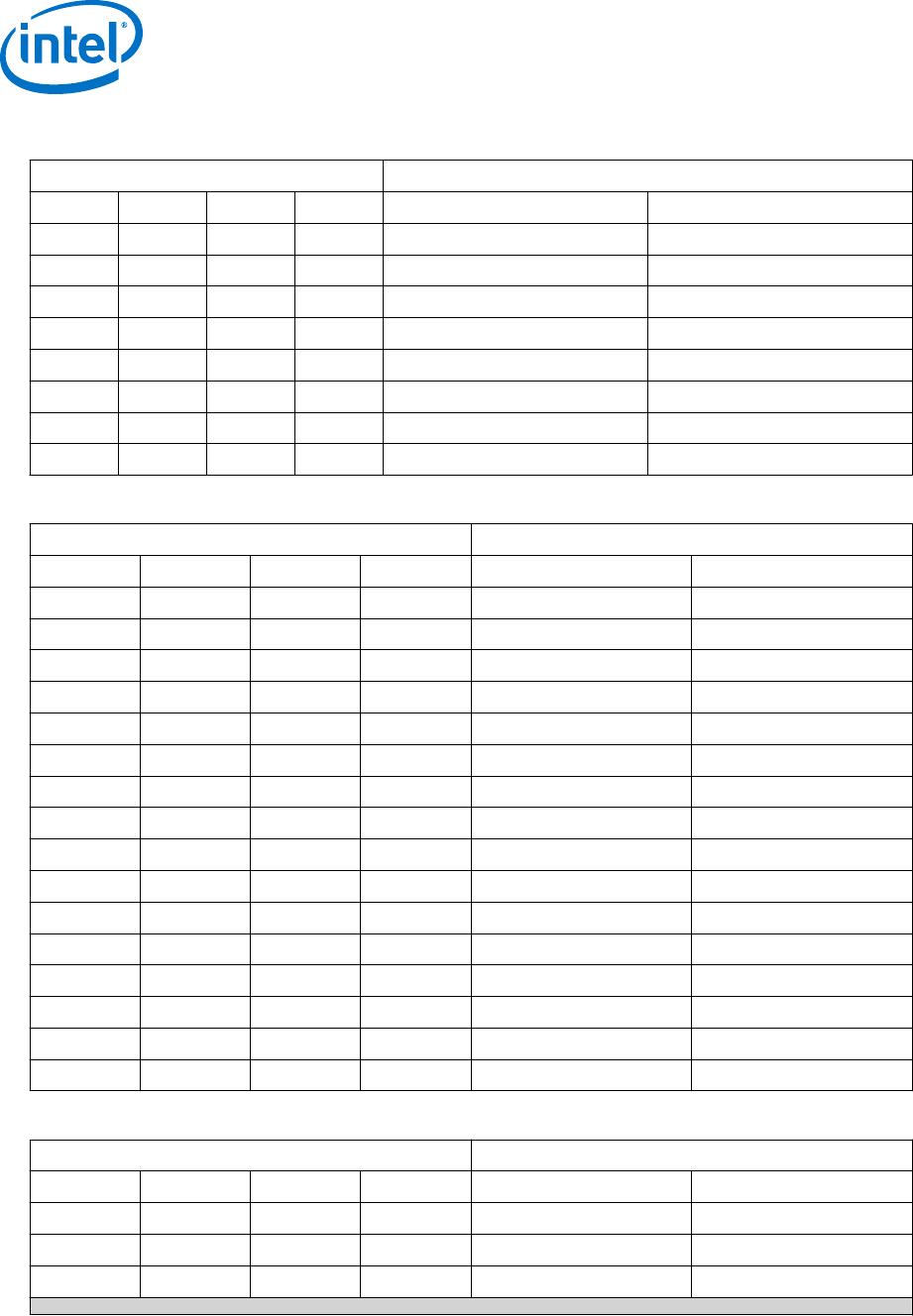
Table 18. Block Protection Bits in EPCQ16A
Status Register Content Memory Content
TB Bit BP2 Bit BP1 Bit BP0 Bit Protected Area Unprotected Area
0 0 0 0 None All sectors
0 0 0 1 Sector 31 Sectors (0 to 30)
0 0 1 0 Sectors (30 to 31) Sectors (0 to 29)
0 0 1 1 Sectors (28 to 31) Sectors (0 to 27)
0 1 0 0 Sectors (24 to 31) Sectors (0 to 23)
0 1 0 1 Sectors (16 to 31) Sectors (0 to 15)
0 1 1 0 All sectors None
0 1 1 1 All sectors None
1 0 0 0 None All sectors
1 0 0 1 Sector 0 Sectors (1 to 31)
1 0 1 0 Sectors (0 to 1) Sectors (2 to 31)
1 0 1 1 Sectors (0 to 3) Sectors (4 to 31)
1 1 0 0 Sectors (0 to 7) Sectors (8 to 31)
1 1 0 1 Sectors (0 to 15) Sectors (16 to 31)
1 1 1 0 All sectors None
1 1 1 1 All sectors None
Table 19. Block Protection Bits in EPCQ32A
Status Register Content Memory Content
TB Bit BP2 Bit BP1 Bit BP0 Bit Protected Area Unprotected Area
0 0 0 0 None All sectors
0 0 0 1 Sector 63 Sectors (0 to 62)
0 0 1 0 Sectors (62 to 63) Sectors (0 to 61)
continued...
1. EPCQ-A Serial Configuration Device Datasheet
CF52014 | 2018.04.11
EPCQ-A Serial Configuration Device Datasheet
18

EPCQ64ASI16N

Mfr. #:
Manufacturer:
Intel / Altera
Description:
FPGA - Configuration Memory
Lifecycle:
New from this manufacturer.
Delivery:
DHL FedEx Ups TNT EMS
Payment:
T/T Paypal Visa MoneyGram Western Union