Note: This operation is applicable to EPCQ4A, EPCQ16A and EPCQ64A devices only.
The device implements the read silicon ID operation by driving the nCS signal low and
then shifting in the read silicon ID operation code, followed by three dummy bytes on
the DATA0 pin. The 8-bit silicon ID of the EPCQ-A device is then shifted out on the
DATA1 pin at falling edges of the DCLK signal. The device can terminate the read
silicon ID operation by driving the nCS signal high after reading the silicon ID at least
one time. Sending additional clock cycles on DCLK while nCS is driven low can cause
the silicon ID to be shifted out repeatedly.
Table 23. EPCQ-A Silicon Identification
EPCQ-A Device Silicon ID (Binary Value)
EPCQ4A
b'0001 0010
EPCQ16A
b'0001 0100
EPCQ64A
b'0001 0110
Figure 11. Read Silicon Identification Operation Timing Diagram
nCS
DCLK
DATA0
DATA1
0 1 2 3 4 5 6 7 8 9 10 28 29 30 31 32 33 34 35 36 37 38
Operation Code (ABh) Three Dummy Bytes
23
22 21
3 2 1 0
7 6 5 4 3 2 1 0
MSB
MSB
High Impedance
Silicon ID
1.9.7. Write Enable Operation (06h)
When you enable the write enable operation, the write enable latch bit is set to 1 in
the status register. You must execute this operation before the write bytes, write
status, erase bulk, erase sector, and quad input fast write bytes operations.
Figure 12. Write Enable Operation Timing Diagram
nCS
DCLK
DATA0
DATA[3:1]
Operation Code (06h)
High Impedance
0 1 2 3 4 5 6 7
1. EPCQ-A Serial Configuration Device Datasheet
CF52014 | 2018.04.11
EPCQ-A Serial Configuration Device Datasheet
25
1.9.8. Write Disable Operation (04h)
The write disable operation resets the write enable latch bit in the status register. To
prevent the memory from being written unintentionally, the write enable latch bit is
automatically reset when implementing the write disable operation, and under the
following conditions:
Power up
Write bytes operation completion
Write status operation completion
Erase bulk operation completion
Erase sector operation completion
Quad input fast write bytes operation completion
Figure 13. Write Disable Operation Timing Diagram
Operation Code (04h)
DATA0
nCS
DCLK
DATA[3:1]
High Impedance
0
1
2
3
4
5
6
7
1.9.9. Write Bytes Operation (02h)
This operation allows bytes to be written to the memory. You must execute the write
enable operation before the write bytes operation. After the write bytes operation is
completed, the write enable latch bit in the status register is set to 0.
When you execute the write bytes operation, you shift in the write bytes operation
code, followed by a 3-byte address (A[23..0]) and at least one data byte on the
DATA0 pin. If the eight LSBs (A[7..0]) are not all 0, all sent data that goes beyond
the end of the current page is not written into the next page. Instead, this data is
written at the start address of the same page. You must ensure the nCS signal is set
low during the entire write bytes operation.
Figure 14. Write Bytes Operation Timing Diagram
DATA0
Operation Code (02h)
24-Bit Address Data Byte 1 Data Byte 2 Data Byte 256
0
1
2
3
4
5
6
7
8
9
10
28
29
30
31
32
nCS
DCLK
33
34
35
36
37 38
39
40
41
42 43
44
45
46
47
3 2 1 0 7 6 5 4 3 2 1 0 7 6 5 4 3 2 1 023 22 21 7 6 5 4 3 2 1 0
2072
2073
2074 2075
2076
2077
2078
2079
MSB MSB MSB MSB
1. EPCQ-A Serial Configuration Device Datasheet
CF52014 | 2018.04.11
EPCQ-A Serial Configuration Device Datasheet
26
If more than 256 data bytes are shifted into the EPCQ-A device with a write bytes
operation, the previously latched data is discarded and the last 256 bytes are written
to the page. However, if less than 256 data bytes are shifted into the EPCQ-A device,
they are guaranteed to be written at the specified addresses and the other bytes of
the same page are not affected.
The device initiates a self-timed write cycle immediately after the nCS signal is driven
high. For details about the self-timed write cycle time, refer to t
WB
in the related
information below. You must account for this amount of delay before another page of
memory is written. Alternatively, you can check the write in progress bit in the status
register by executing the read status operation while the self-timed write cycle is in
progress. The write in progress bit is set to 1 during the self-timed write cycle and 0
when it is complete.
Note: You must erase all the memory bytes of EPCQ-A devices before you implement the
write bytes operation. You can erase all the memory bytes by executing the erase
sector operation in a sector or the erase bulk operation throughout the entire memory
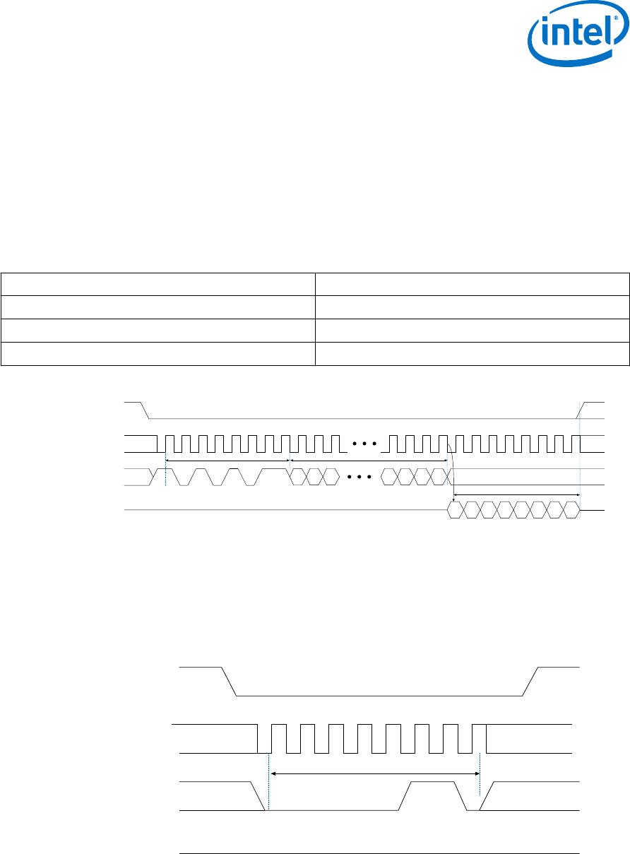
1.9.10. Quad Input Fast Write Bytes Operation (32h)
This operation is similar to the write bytes operation except that the data are shifted
in on the DATA0, DATA1, DATA2, and DATA3 pins.
Figure 15. Quad Input Fast Write Bytes Operation Timing Diagram
DATA0
DATA1
nCS
Operation Code (32h)
High Impedance
MSB
DATA2
DATA3
High Impedance
High Impedance
Data In
21 3 9 100
DCLK
3734
35
36
30
31
32
33
39
38
40
42
41
43
MSB
MSBMSB
MSB
MSB
24-bit Address
Data In Data In
2
1 3 4
5
6
44
23 22
21
0 4
1 0
4
0
4
0
4
0
4 40
0 4
0
2 6
6
2
6
2
6
2
6 62
2 6
2
1 5
5
1
5
1
5
1
5 51
1 5
1
3 7
7
3
7
3
7
3
7 73
3 7
3
7
MSB
4
65 7
8
45
1.9.11. Erase Bulk Operation (C7h)
This operation sets all the memory bits to 1 or 0xFF. Similar to the write bytes
operation, you must execute the write enable operation before the erase bulk
operation.
You can implement the erase bulk operation by driving the nCS signal low and then
shifting in the erase bulk operation code on the DATA0 pin. The nCS signal must be
driven high after the eighth bit of the erase bulk operation code has been latched in.
1. EPCQ-A Serial Configuration Device Datasheet
CF52014 | 2018.04.11
EPCQ-A Serial Configuration Device Datasheet
27

EPCQ64ASI16N

Mfr. #:
Manufacturer:
Intel / Altera
Description:
FPGA - Configuration Memory
Lifecycle:
New from this manufacturer.
Delivery:
DHL FedEx Ups TNT EMS
Payment:
T/T Paypal Visa MoneyGram Western Union