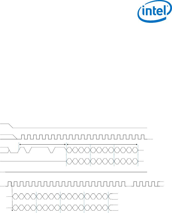
the content is shifted out serially beginning with the LSB. Each data bit is shifted out
at falling edges of the DCLK signal. The maximum DCLK frequency during the read
bytes operation is 50 MHz.
Figure 6. Read Bytes Operation Timing Diagram
nCS
DCLK
DATA0
DATA1
0 1 2 3 4 5 6 7 8 9 10 28 29 30 31 32 33 34 35 36 37 38 39
Operation Code (03h) 24-Bit Address
23 22 21 3 2 1 0
7 76 5 4 3 2 1 0
MSB
MSB
High Impedance
DATA Out 1 DATA Out 2
The first byte address can be at any location. The device automatically increases the
address to the next higher address after shifting out each byte of data. Therefore, the
device can read the whole memory with a single read bytes operation. When the
device reaches the highest address, the address counter restarts at 0x000000,
allowing the memory contents to be read out indefinitely until the read bytes
operation is terminated by driving the nCS signal high. If the read bytes operation is
shifted in while a write or erase cycle is in progress, the operation is not executed and
does not affect the write or erase cycle in progress.
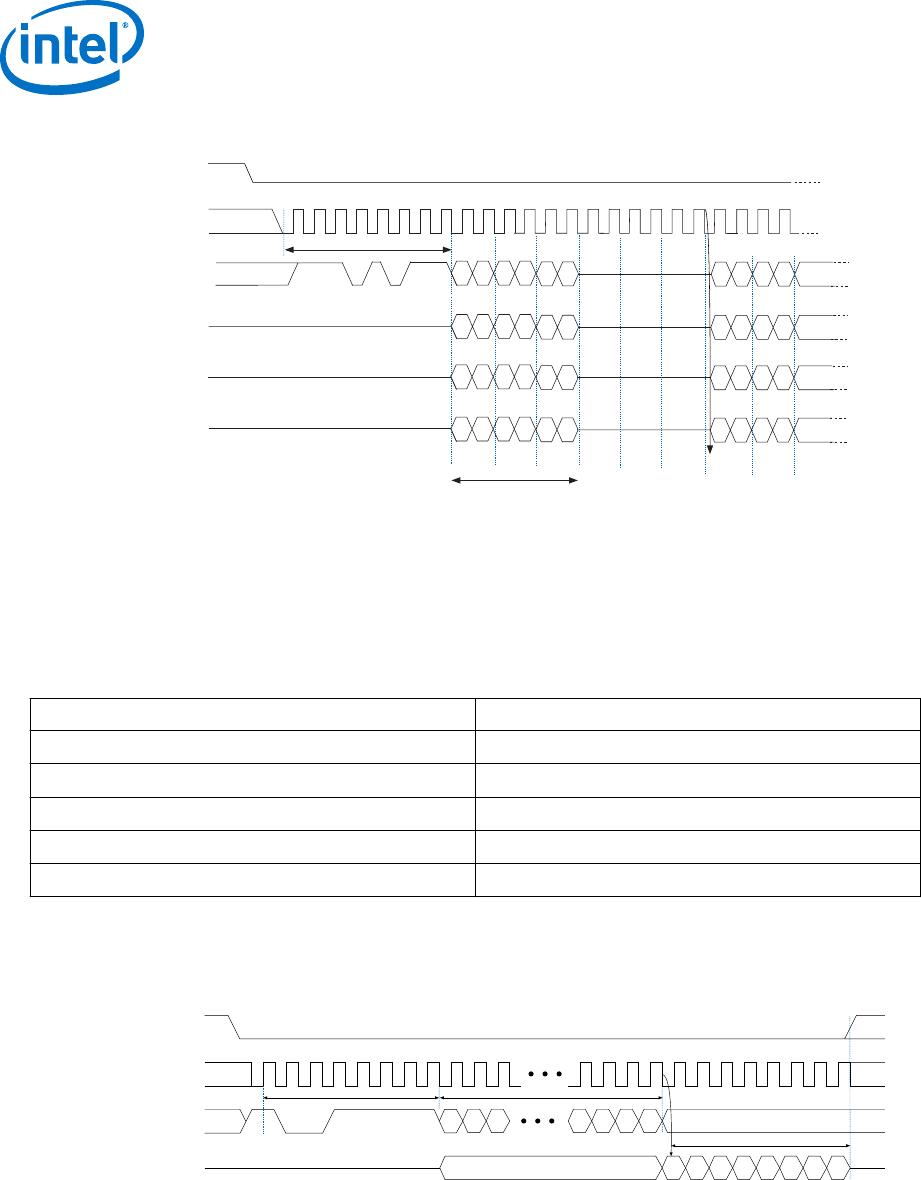
1.9.2. Fast Read Operation (0Bh)
When you execute the fast read operation, you first shift in the fast read operation
code, followed by a 3-byte address (A[23..0]), and 8 dummy cycles with each bit
being latched-in at rising edges of the DCLK signal. Then, the memory contents at that
address is shifted out on DATA1 with each bit being shifted out at a maximum
frequency of 100 MHz at falling edges of the DCLK signal.
Figure 7. Fast Read Operation Timing Diagram
nCS
DCLK
DATA0
DATA1
nCS
DCLK
DATA0
DATA1
0 1 2 3 4 5 6 7 8 9 10 28 29 30 31
Operation Code (0Bh)
8 Dummy Cycles
24-Bit Address
MSB
MSB MSB MSB
High Impedance
23 22 21 3 2 1 0
Byte1 Byte 2
32 33 34 35 36 37 38 39 40 41 42 43 44 45 46 47
7 6 5 4 3 2 1 0 7 6 5 4 3 2 1 0 7
7 6 5 4 3 2 1 0
1. EPCQ-A Serial Configuration Device Datasheet
CF52014 | 2018.04.11
EPCQ-A Serial Configuration Device Datasheet
22