Status Register Content Memory Content
TB Bit BP2 Bit BP1 Bit BP0 Bit Protected Area Unprotected Area
0 0 1 1 Sectors (60 to 63) Sectors (0 to 59)
0 1 0 0 Sectors (56 to 63) Sectors (0 to 55)
0 1 0 1 Sectors (48 to 63) Sectors (0 to 47)
0 1 1 0 Sectors (32 to 63) Sectors (0 to 31)
0 1 1 1 All sectors None
1 0 0 0 None All sectors
1 0 0 1 Sector 0 Sectors (1 to 63)
1 0 1 0 Sectors (0 to 1) Sectors (2 to 63)
1 0 1 1 Sectors (0 to 3) Sectors (4 to 63)
1 1 0 0 Sectors (0 to 7) Sectors (8 to 63)
1 1 0 1 Sectors (0 to 15) Sectors (16 to 63)
1 1 1 0 Sectors (0 to 31) Sectors (32 to 63)
1 1 1 1 All sectors None
Table 20. Block Protection Bits in EPCQ64A
Status Register Content Memory Content
TB Bit BP2 Bit BP1 Bit BP0 Bit Protected Area Unprotected Area
0 0 0 0 None All sectors
0 0 0 1 Sectors (126 to 127) Sectors (0 to 125)
0 0 1 0 Sectors (124 to 127) Sectors (0 to 123)
0 0 1 1 Sectors (120 to 127) Sectors (0 to 119)
0 1 0 0 Sectors (112 to 127) Sectors (0 to 111)
0 1 0 1 Sectors (96 to 127) Sectors (0 to 95)
0 1 1 0 Sectors (64 to 127) Sectors (0 to 63)
0 1 1 1 All sectors None
1 0 0 0 None All sectors
1 0 0 1 Sectors (0 to 1) Sectors (2 to 127)
1 0 1 0 Sectors (0 to 3) Sectors (4 to 127)
1 0 1 1 Sectors (0 to 7) Sectors (8 to 127)
1 1 0 0 Sectors (0 to 15) Sectors (16 to 127)
1 1 0 1 Sectors (0 to 31) Sectors (32 to 127)
1 1 1 0 Sectors (0 to 63) Sectors (64 to 127)
1 1 1 1 All sectors None
1. EPCQ-A Serial Configuration Device Datasheet
CF52014 | 2018.04.11
EPCQ-A Serial Configuration Device Datasheet
19
Table 21. Block Protection Bits in EPCQ128A
Status Register Content Memory Content
TB Bit BP2 Bit BP1 Bit BP0 Bit Protected Area Unprotected Area
0 0 0 0 None All sectors
0 0 0 1 Sectors (252 to 255) Sectors (0 to 251)
0 0 1 0 Sectors (248 to 255) Sectors (0 to 247)
0 0 1 1 Sectors (240 to 255) Sectors (0 to 239)
0 1 0 0 Sectors (224 to 255) Sectors (0 to 223)
0 1 0 1 Sectors (192 to 255) Sectors (0 to 191)
0 1 1 0 Sectors (128 to 255) Sectors (0 to 127)
0 1 1 1 All sectors None
1 0 0 0 None All sectors
1 0 0 1 Sectors (0 to 3) Sectors (4 to 255)
1 0 1 0 Sectors (0 to 7) Sectors (8 to 255)
1 0 1 1 Sectors (0 to 15) Sectors (16 to 255)
1 1 0 0 Sectors (0 to 31) Sectors (32 to 255)
1 1 0 1 Sectors (0 to 63) Sectors (64 to 255)
1 1 1 0 Sectors (0 to 127) Sectors (128 to 255)
1 1 1 1 All sectors None
1.8.2. Write Status Operation
The write status operation does not affect the write enable latch and write in progress
bits. You can use the write status operation to set the status register block protection
and top or bottom bits. Therefore, you can implement this operation to protect certain
memory sectors. After setting the block protect bits, the protected memory sectors
are treated as read-only memory. You must execute the write enable operation before
the write status operation.
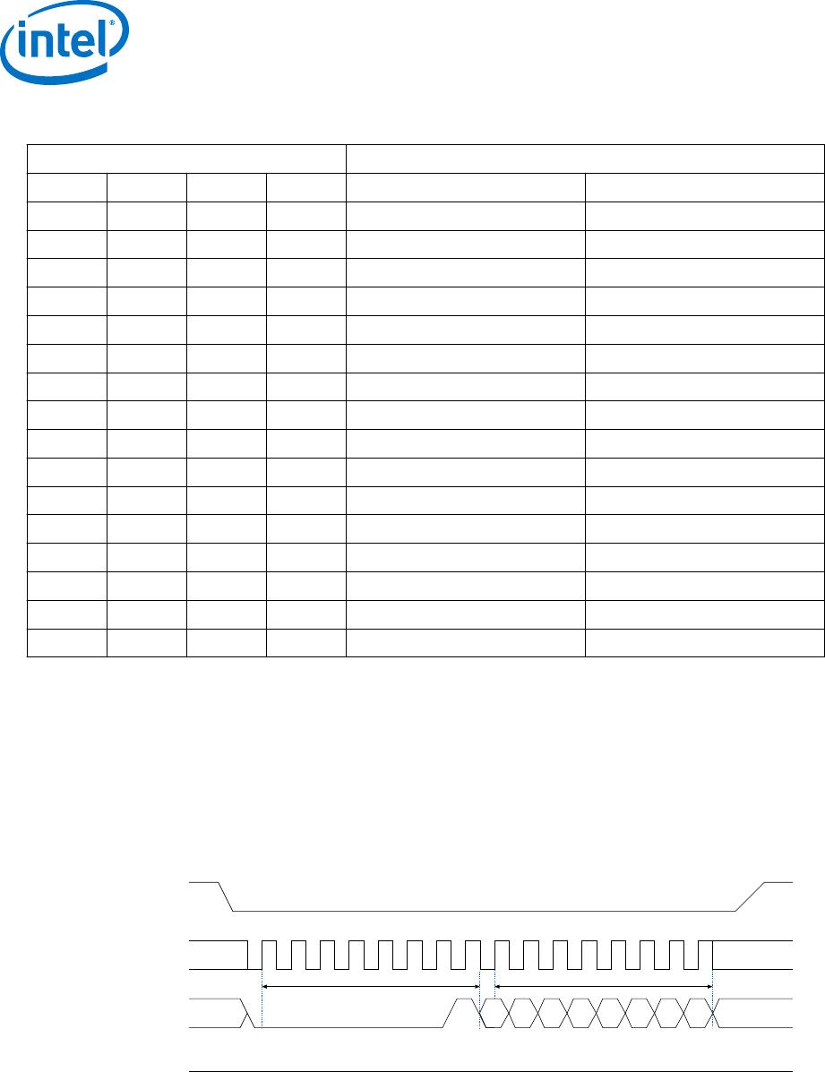
Figure 5. Write Status Operation Timing Diagram
Operation Code (01h) Status Register
DATA0
nCS
DCLK
DATA
High Impedance
0
1
2
3
4
5
6
7
8 9 10 11 12 13 14 15
0
1
2
3
4
5
6
7
MSB
Immediately after the nCS signal drives high, the device initiates the self-timed write
status cycle. The self-timed write status cycle usually takes 10 ms for all EPCQ-A
devices and is guaranteed to be less than 15 ms. For details about t
WS
, refer to the
related information below. You must account for this delay to ensure that the status
register is written with the desired block protect bits. Alternatively, you can check the
1. EPCQ-A Serial Configuration Device Datasheet
CF52014 | 2018.04.11
EPCQ-A Serial Configuration Device Datasheet
20
write in progress bit in the status register by executing the read status operation while
the self-timed write status cycle is in progress. Write in progress bit is 1 during the
self-timed write status cycle and 0 when it is complete.
1.9. Summary of Operation Codes
Operation Operation Code
(7)
Address Bytes Dummy Cycles Data Bytes DCLK f
MAX
(MHz)
Read status
05h
0 0 1 to infinite
(8)
100
Read bytes
03h
3 0 1 to infinite
(8)
50
Read device identification
9Fh
0 2 1 100
Read silicon identification
ABh
0 3 1 100
Fast read
0Bh
3 8 1 to infinite
(8)
100
Extended dual input fast
read
BBh
3 4 1 to infinite
(8)
100
Extended quad input fast
read
(9)
EBh
3 6 1 to infinite
(8)
100
Write enable
06h
0 0 0 100
Write disable
04h
0 0 0 100
Write status
01h
0 0 1 100
Write bytes
02h
3 0 1 to 256
(10)
100
Quad input fast write
bytes
(9)
32h
3 0 1 to 256
(10)
100
Erase bulk
C7h
0 0 0 100
Erase sector
D8h
3 0 0 100
Erase subsector
20h
3 0 0 100
Read SFDP register
(9)
5Ah
3 8 1 to 256 100
1.9.1. Read Bytes Operation (03h)
When you execute the read bytes operation, you first drive the nCS pin low and shift
in the read bytes operation code, followed by a 3-byte address (A[23..0]). Each
address bit must be latched in at rising edges of the DCLK signal. After the address is
latched in, the memory contents of the specified address are shifted out serially on the
DATA1 pin, beginning with the MSB. For reading Raw Programming Data File (.rpd),
(7)
List MSB first and LSB last.
(8)
The status register or data is read out at least once and is continuously read out until the nCS
pin is driven high.
(9)
This operation is not applicable for EPCQ4A.
(10)
A write bytes operation requires at least one data byte. If more than 256 bytes are sent to the
device, only the last 256 bytes are written to the memory.
1. EPCQ-A Serial Configuration Device Datasheet
CF52014 | 2018.04.11
EPCQ-A Serial Configuration Device Datasheet
21

EPCQ64ASI16N

Mfr. #:
Manufacturer:
Intel / Altera
Description:
FPGA - Configuration Memory
Lifecycle:
New from this manufacturer.
Delivery:
DHL FedEx Ups TNT EMS
Payment:
T/T Paypal Visa MoneyGram Western Union