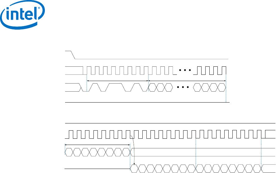
Figure 16. Erase Bulk Operation Timing Diagram
Operation Code (C7h)
DATA0
nCS
DCLK
0 1
2
3 4
5
6 7
The device initiates a self-timed erase bulk cycle immediately after the nCS signal is
driven high. For details about the self-timed erase bulk cycle time, refer to t
EB
in the
related information below.
You must account for this delay before accessing the memory contents. Alternatively,
you can check the write in progress bit in the status register by executing the read
status operation while the self-timed erase cycle is in progress. The write in progress
bit is set to 1 during the self-timed erase cycle and 0 when it is complete. The write
enable latch bit in the status register is reset to 0 before the erase cycle is complete.
1.9.12. Erase Sector Operation (D8h)
The erase sector operation allows you to erase a certain sector in the EPCQ-A device
by setting all the bits inside the sector to 1 or 0xFF. This operation is useful if you
want to access the unused sectors as a general purpose memory in your applications.
You must execute the write enable operation before the erase sector operation.
When you execute the erase sector operation, you must first shift in the erase sector
operation code, followed by the 3-byte address (A[23..0]) of the chosen sector on
the DATA0 pin. The 3-byte address for the erase sector operation can be any address
inside the specified sector. Drive the nCS signal high after the eighth bit of the erase
sector operation code has been latched in.
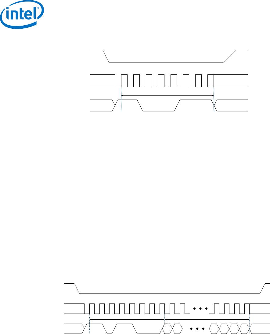
Figure 17. Erase Sector Operation Timing Diagram
DATA0
Operation Code (D8h) 24-Bit Address
nCS
DCLK
0 1 2 3 4 5 6 7 8 9 28 29 30 31
3 2
1 023 22
MSB
The device initiates a self-timed erase sector cycle immediately after the nCS signal is
driven high. For details about the self-timed erase sector cycle time, refer to t
ES
in the
related information below. You must account for this amount of delay before another
page of memory is written. Alternatively, you can check the write in progress bit in the
status register by executing the read status operation while the self-timed erase cycle
is in progress. The write in progress bit is set to 1 during the self-timed erase cycle
and 0 when it is complete. The write enable latch bit in the status register is set to 0
before the self-timed erase cycle is complete.
1. EPCQ-A Serial Configuration Device Datasheet
CF52014 | 2018.04.11
EPCQ-A Serial Configuration Device Datasheet
28
1.9.13. Erase Subsector Operation (20h)
The erase subsector operation allows you to erase a certain subsector in the EPCQ-A
device by setting all the bits inside the subsector to 1 or 0xFF. This operation is useful
if you want to access the unused subsectors as a general purpose memory in your
applications. You must execute the write enable operation before the erase subsector
operation.
When you execute the erase subsector operation, you must first shift in the erase
subsector operation code, followed by the 3-byte address (A[23..0]) of the chosen
subsector on the DATA0 pin. The 3-byte address for the erase subsector operation can
be any address inside the specified subsector. For details about the subsector address
range, refer to the related information below. Drive the nCS signal high after the
eighth bit of the erase subsector operation code has been latched in.
Figure 18. Erase Subsector Operation Timing Diagram
DATA0
Operation Code (20h) 24-Bit Address
nCS
DCLK
0 1 2 3 4 5 6 7 8 9 28 29 30 31
3 2
1 023 22
MSB
The device initiates a self-timed erase subsector cycle immediately after the nCS
signal is driven high. For details about the self-timed erase subsector cycle time, refer
to related the information below. You must account for this amount of delay before
another page of memory is written. Alternatively, you can check the write in progress
bit in the status register by executing the read status operation while the self-timed
erase cycle is in progress. The write in progress bit is set to 1 during the self-timed
erase cycle and 0 when it is complete. The write enable latch bit in the status register
is set to 0 before the self-timed erase cycle is complete.
1.9.14. Read SFDP Register Operation (5Ah)
The 256-byte SFDP register contains information about device configurations,
available operations and other features.
The Read SFDP Register operation is compatible with the JEDEC SFDP standard,
JESD216A. For SFDP register values and descriptions, please refer to Appendix: SFDP
Register Definitions on page 34.
1. EPCQ-A Serial Configuration Device Datasheet
CF52014 | 2018.04.11
EPCQ-A Serial Configuration Device Datasheet
29
Figure 19. Read SFDP Register Operation Timing Diagram
nCS
DCLK
DATA0
DATA1
nCS
DCLK
DATA0
DATA1
0 1 2 3 4 5 6 7 8 9 10 28 29 30 31
Operation Code (5Ah)
8 Dummy Cycles
24-Bit Address
MSB
MSB MSB MSB
High Impedance
23 22 21 3 2 1 0
Byte 0 Byte 1
32 33 34 35 36 37 38 39 40 41 42 43 44 45 46 47
7 6 5 4 3 2 1 0 7 6 5 4 3 2 1 0 7
7 6 5 4 3 2 1 0
Initiate the Read SFDP operation by driving the nCS pin low and shifting the
operations code followed by a 3-byte address into the DATA0 pin. The 3-byte address
content:
A[23..8] = 0
A[7..0] = Defines the starting byte address for the 256-byte SFDP register
Eight dummy cycles are required before the SFDP register contents are shifted out on
the falling edge of the 40
th
DCLK with the most significant bit (MSB) first.
Related Information
Appendix: SFDP Register Definitions on page 34
1.10. Power Mode
EPCQ-A devices support active and standby power modes. When the nCS signal is low,
the device is enabled and is in active power mode. The FPGA is configured while the
EPCQ-A device is in active power mode. When the nCS signal is high, the device is
disabled but remains in active power mode until all internal cycles are completed, such
as write or erase operations. The EPCQ-A device then goes into standby power mode.
The I
CC1
and I
CC0
parameters list the V
CC
supply current when the device is in active
and standby power modes.
1. EPCQ-A Serial Configuration Device Datasheet
CF52014 | 2018.04.11
EPCQ-A Serial Configuration Device Datasheet
30

EPCQ64ASI16N

Mfr. #:
Manufacturer:
Intel / Altera
Description:
FPGA - Configuration Memory
Lifecycle:
New from this manufacturer.
Delivery:
DHL FedEx Ups TNT EMS
Payment:
T/T Paypal Visa MoneyGram Western Union