PCA8561 All information provided in this document is subject to legal disclaimers. © NXP Semiconductors N.V. 2015. All rights reserved.
Product data sheet Rev. 4 — 27 March 2015 10 of 55
NXP Semiconductors
PCA8561
Automotive 18 × 4 LCD segment driver
8.3 Starting and resetting the PCA8561
If the internal Power-On Reset (POR) is enabled by connecting pin PORE to V
DD
, the chip
resets automatically when V
DD
rises above the minimum supply voltage. No further action
is required.
If the internal POR is disabled by connecting pin PORE to V
SS
, the chip must be reset by
driving the RST
pin to logic 0 for at least 10 s, see Figure 6.
Alternatively a software reset can be applied (see Section 8.3.4).
Following a reset, the register 00h has to be rewritten with 0h by the next command byte
or the address pointer AP[4:0] has to be set to the required address after a new START
procedure.
8.3.1 Power-down mode
After a reset, the PCA8561 remains in power-down mode. In power-down mode the
oscillator is switched off and there is no output on pin CLK. The register settings remain
unchanged and the bus remains active. To enable the PCA8561, bit DE (command
Display_ctrl_1, see Table 7 on page 8
) must be set to logic 1.
8.3.2 Power-On Reset (POR)
If pin PORE is connected to V
DD
, the PCA8561 comprises an internal POR, which puts
the device into the following starting conditions:
All backplane and segment outputs are set to V
SS
The selected drive mode is: 1:4 multiplex with
1
3
bias
Blinking is switched off
The address pointer is cleared (set to logic 0)
The display and the internal oscillator are disabled
The display registers are set to logic 0
The bus interface is initialized
Fig 6. Reset pulse timing
W
ZUVW
 V
PLQLPXP
W
ZUVW
 V
PLQLPXP
9
''PLQ
9
'
'
567
9DOLGUHVHWSXOVH
GXULQJSRZHUXS
9DOLGUHVHWSXOVH
DIWHUSRZHUXS
DDD
PCA8561 All information provided in this document is subject to legal disclaimers. © NXP Semiconductors N.V. 2015. All rights reserved.
Product data sheet Rev. 4 — 27 March 2015 11 of 55
NXP Semiconductors
PCA8561
Automotive 18 × 4 LCD segment driver
Remark: The internal POR can be disabled by connecting pin PORE to V
SS
. In this case,
the internal registers are not defined and require a hardware reset according to
Section 8.3.3
or a software reset, see Section 8.3.4.
8.3.3 Hardware reset: RST pin
At power-on the PCA8561 can be reset to the following starting conditions by pulling pin
RST
low:
All backplane and segment outputs are set to V
SS
The selected drive mode is: 1:4 multiplex with
1
3
bias
Blinking is switched off
The bus interface is initialized
The address pointer is cleared (set to logic 0)
The display and the internal oscillator are disabled
The display registers are set to logic 0
Remark: The hardware reset overrides the POR see Section 8.3.2
.
8.3.4 Command: Software_reset
The internal registers including the display registers and the address pointer (set to
logic 0) of the device are reset by the Software_reset command.
[1] Default value.
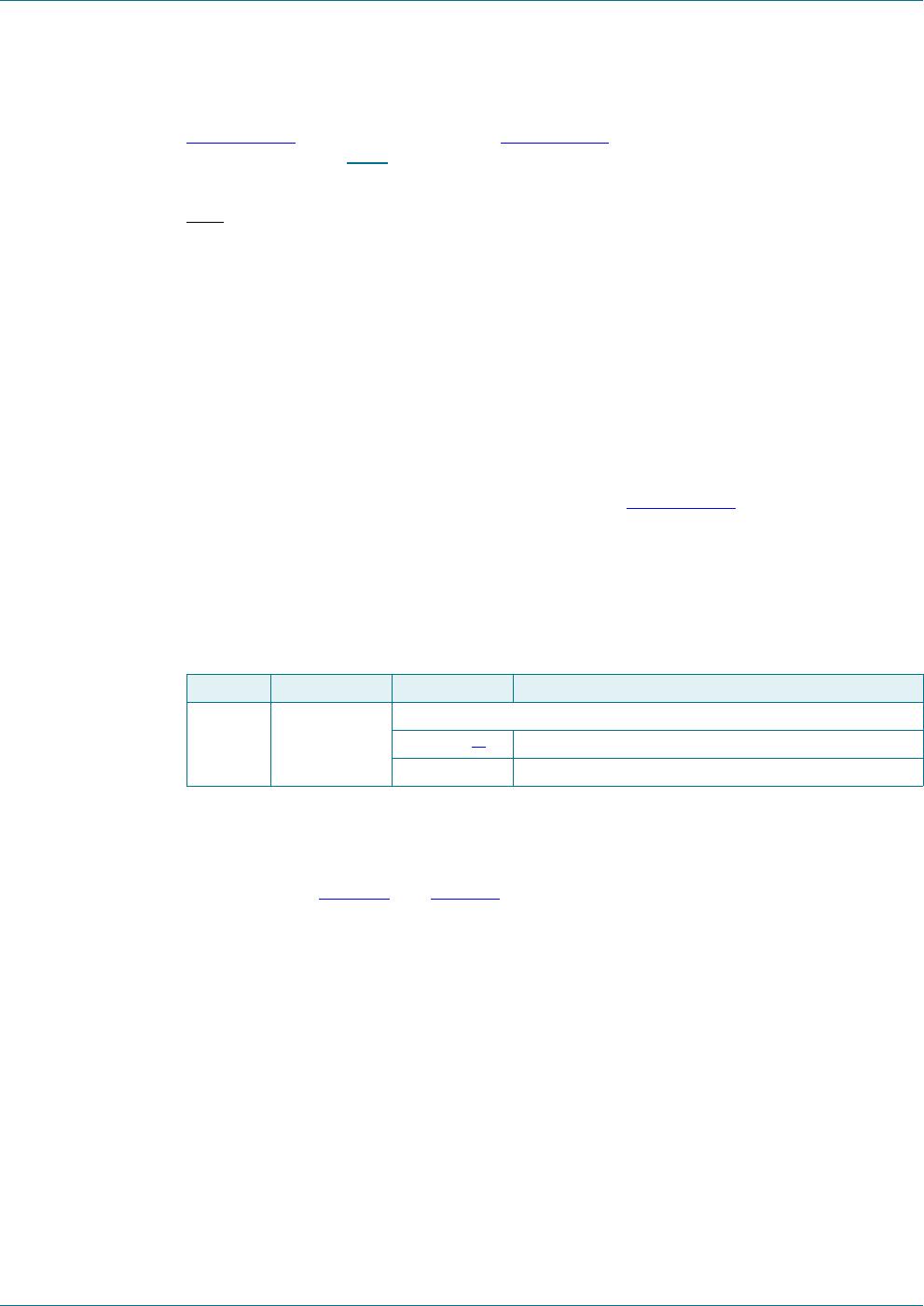
8.4 Display data register mapping
The example in Table 10 and Figure 7 illustrates the segment and backplane mapping of
the display in relation to the display RAM.
For example, in 1:4 multiplex drive mode, the backplanes are served by signals COM0 to
COM3 and the segments are driven by signals SEG0 to SEG17. Contents of addresses
04h to 06h are allocated to the first row (COM0) starting with the LSB driving the leftmost
element and moving forward to the right with increasing bit position. If a bit is logic 0, the
element is off, if it is logic 1 the element is turned on. All register content is LSB to MSB
left to right. Addresses 07h to 09h serve COM1 signals, addresses 0Ah to 0Ch serve
COM2 signals, and addresses 0Dh to 0Fh serve COM3 signals.
For displays with fewer segments/elements the unused bits are ignored.
Table 9. Software_reset - software reset command register (address 00h) bit description
This register can only be written but not read.
Bit Symbol Value Description
7 to 0 SR[7:0] software reset
00000000
[1]
no reset
00101100 software reset
PCA8561 All information provided in this document is subject to legal disclaimers. © NXP Semiconductors N.V. 2015. All rights reserved.
Product data sheet Rev. 4 — 27 March 2015 12 of 55
NXP Semiconductors
PCA8561
Automotive 18 × 4 LCD segment driver
[1] See also Section 9.3.1 on page 23.
[2] Bits [7:2] are ignored.
Table 10. Register to segment and backplane mapping
Backplanes
[1]
Segments
SEG0 to SEG7 SEG8 to SEG15 SEG16 to SEG17
LSB MSB LSB MSB LSB MSB
1:4 multiplex drive mode
COM0 content of 04h content of 05h content of 06h
[2]
COM1 content of 07h content of 08h content of 09h
[2]
COM2 content of 0Ah content of 0Bh content of 0Ch
[2]
COM3 content of 0Dh content of 0Eh content of 0Fh
[2]
1:3 multiplex drive mode
COM0 content of 04h content of 05h content of 06h
[2]
COM1 content of 07h content of 08h content of 09h
[2]
COM2 content of 0Ah content of 0Bh content of 0Ch
[2]
1:2 multiplex drive mode
COM0 content of 04h content of 05h content of 06h
[2]
COM1 content of 07h content of 08h content of 09h
[2]
static drive mode
COM0 content of 04h content of 05h content of 06h
[2]
Fig 7. Display RAM organization bitmap for MUX 1:4
&20
&20
&20
&20
6(*
6(*
6(*
6(*
6(*
6(*
6(*
6(*
6(*
6(*
6(*
6(*
6(*
6(*
6(*
6(*
6(*
6(*
'
'
'
'
'
'
'
'
'
'
'
'
'
'
'
'
'
'
'
'
'
'
'
'
'
'
'
'
5$0
'LVSOD\
DDD
GLVFDUGHG

PCA8561BHN/AY

Mfr. #:
Manufacturer:
NXP Semiconductors
Description:
Equalizers Automotive 18 X 4 LCD segment driver
Lifecycle:
New from this manufacturer.
Delivery:
DHL FedEx Ups TNT EMS
Payment:
T/T Paypal Visa MoneyGram Western Union

Products related to this Datasheet