PCA8561 All information provided in this document is subject to legal disclaimers. © NXP Semiconductors N.V. 2015. All rights reserved.
Product data sheet Rev. 4 — 27 March 2015 5 of 55
NXP Semiconductors
PCA8561
Automotive 18 × 4 LCD segment driver
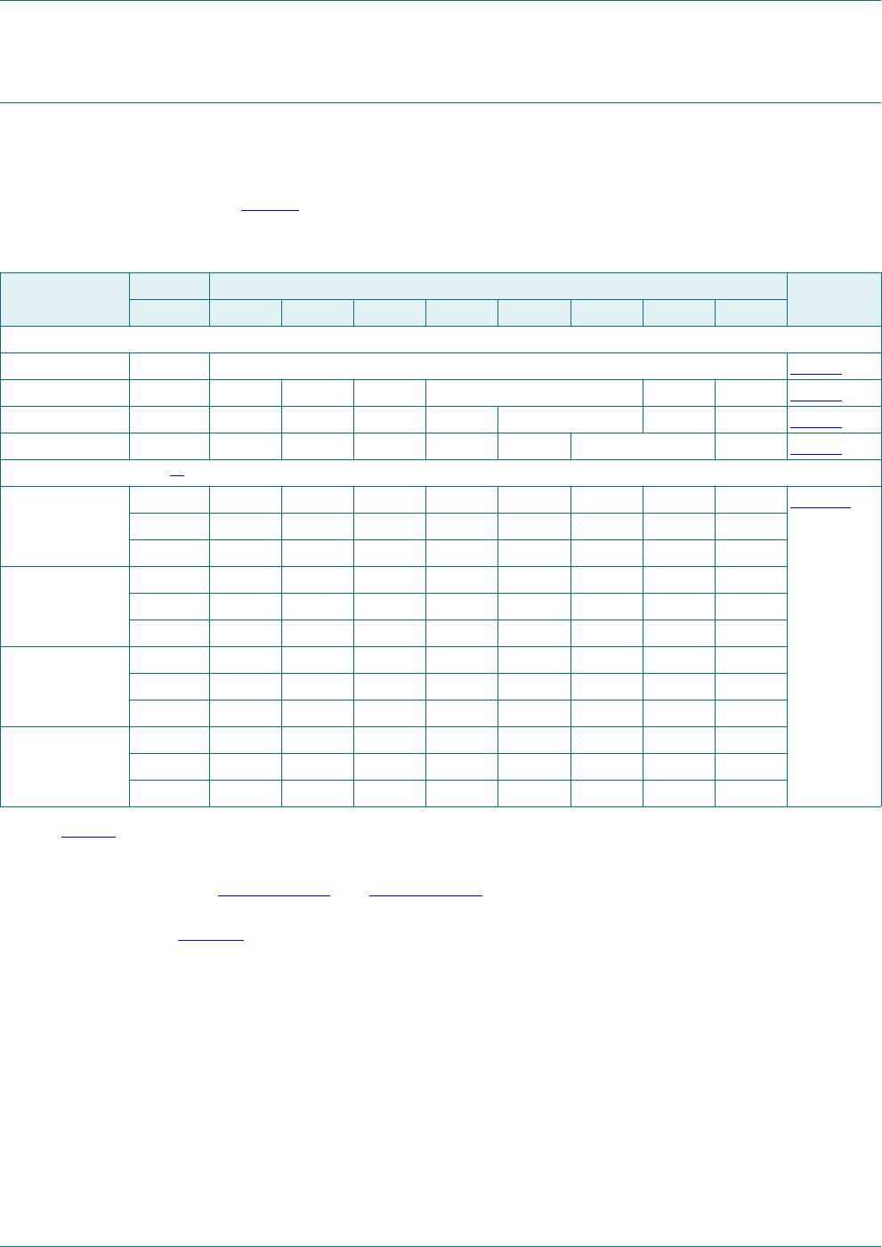
7.2 Pin description
[1] The die paddle (exposed pad) is connected to V
SS
and should be electrically isolated.
[2] A series resistance between V
DD
and the pin must not exceed 1 k to ensure proper functionality, see Section 16.3.
Table 4. Pin description
Input or input/output pins must always be at a defined level (V
SS
or V
DD
) unless otherwise specified.
Pin Symbol Type Description
1 COM3 output LCD backplane output
2 VLCD supply LCD supply voltage
3 VDD supply supply voltage
4 VSS
[1]
supply ground supply
5RST
input reset input, active LOW
7 CLK input/output internal oscillator output, external oscillator input
• must be left open if unused
8 SCL input serial clock input
10 PORE
[2]
input Power-On Reset (POR) enable
• connect to V
DD
for enabling POR
• connect to V
SS
(or leave open) for disabling POR
12 to 29 SEG0 to SEG17 output LCD segment outputs
30 to 32 COM0 to COM2 output LCD backplane outputs
Pin layout depending on product and bus type
PCA8561AHN
(I
2
C-bus)
PCA8561BHN
(SPI-bus)
6A0
[2]
- input hardware device address selection;
• connect to V
SS
(or leave open) for logic 0
• connect to V
DD
for logic 1
- SDIO input/output serial data input/output
9 SDA - output serial data output
-CE
input chip enable input, active LOW
11 A1
[2]
- input hardware device address selection;
• connect to V
SS
(or leave open) for logic 0
• connect to V
DD
for logic 1
- n.c. - not connected