PCA8561 All information provided in this document is subject to legal disclaimers. © NXP Semiconductors N.V. 2015. All rights reserved.
Product data sheet Rev. 4 — 27 March 2015 34 of 55
NXP Semiconductors
PCA8561
Automotive 18 × 4 LCD segment driver
[1] or respectively (see Table 6 and Table 7).
T
amb
=25C; V
LCD
=3.3V; V
DD
= 3.3 V; f
fr
= 64 Hz, BOOST = 0.
(1) Static, all segments/elements off.
(2) Static, all segments/elements on.
(3) MUX 1:2, bias level
1
⁄
2
, all segments/elements off.
(4) MUX 1:2, bias level
1
⁄
2
, all segments/elements on.
(5) MUX 1:3, bias level
1
⁄
3
, all segments/elements off.
(6) MUX 1:3, bias level
1
⁄
3
, all segments/elements on.
(7) MUX 1:4, bias level
1
⁄
3
, all segments/elements off.
(8) MUX 1:4, bias level
1
⁄
3
, all segments/elements on.
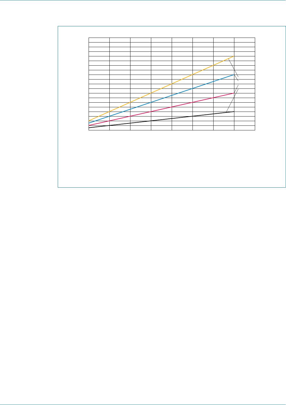
Fig 26. Typical I
DD(LCD)
as function of f
fr
DDD
I
IU
+]
,
''/&'''/&'
,
''/&'
ȝ$ȝ$ȝ$
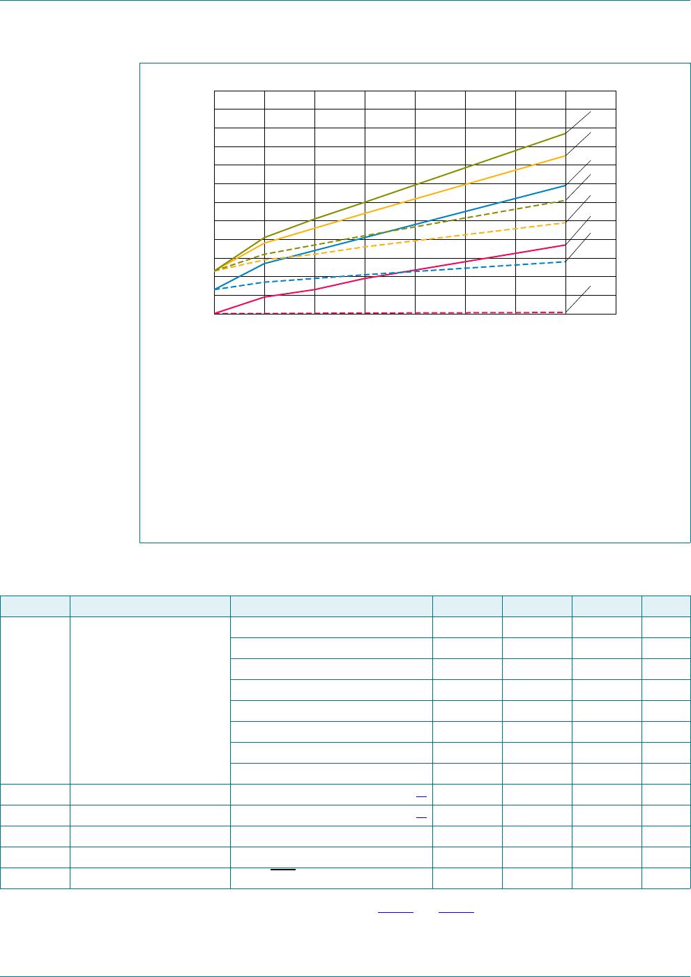
Table 19. Frequency characteristics
V
DD
= 1.8 V to 5.5 V; V
SS
=0V; V
LCD
= 1.8 V to 5.5 V; T
amb
=
40
C to +105
C; unless otherwise specified.
Symbol Parameter Conditions Min Typ Max Unit
f
fr
frame frequency FF[2:0] = 000 - 32 - Hz
FF[2:0] = 001 42 64 86 Hz
FF[2:0] = 010 - 96 - Hz
FF[2:0] = 011 - 128 - Hz
FF[2:0] = 100 - 160 - Hz
FF[2:0] = 101 - 192 - Hz
FF[2:0] = 110 - 224 - Hz
FF[2:0] = 111 - 256 - Hz
f
clk(int)
internal clock frequency f
fr
= 64 Hz, n
MUX
=4
[1]
- 1024 - Hz
f
clk(ext)
external clock frequency
[1]
- - 4096 Hz
t
clk(H)
HIGH-level clock time external clock 60 - - s
t
clk(L)
LOW-level clock time external clock 60 - - s
t
w(rst)
reset pulse width on pin RST 10 - - s
f
clk int
2f
fr
n
MUX
=
f
clk ext
2f
fr
n
MUX
=