PCA8561 All information provided in this document is subject to legal disclaimers. © NXP Semiconductors N.V. 2015. All rights reserved.
Product data sheet Rev. 4 — 27 March 2015 38 of 55
NXP Semiconductors
PCA8561
Automotive 18 × 4 LCD segment driver
16. Application information
16.1 Power-on with a slowly starting power supply
The built-in POR block acts on the rising edge of the V
DD
supply voltage. It is designed to
react to fast slopes. If the system supply starts slowly, it is recommended to initiate a
software reset immediately after power-on.
16.2 I
2
C acknowledge after power-on
If the bus does not show an acknowledge at the first access, the command should be sent
a second time.
16.3 Resistors on I/O pins
The pins A0, A1, and PORE comprise internal, latching pull-down devices, which keep
these inputs at a low potential when left open. If an input is supposed to be at logic 0
potential, this pin can be either connected to V
SS
or left open.
In case a pin is supposed to be at logic 1 potential, it must be connected to V
DD
to avoid
any cross-current during power-up. A series resistance between V
DD
and the associated
pin must not exceed 1 k to ensure proper functionality.
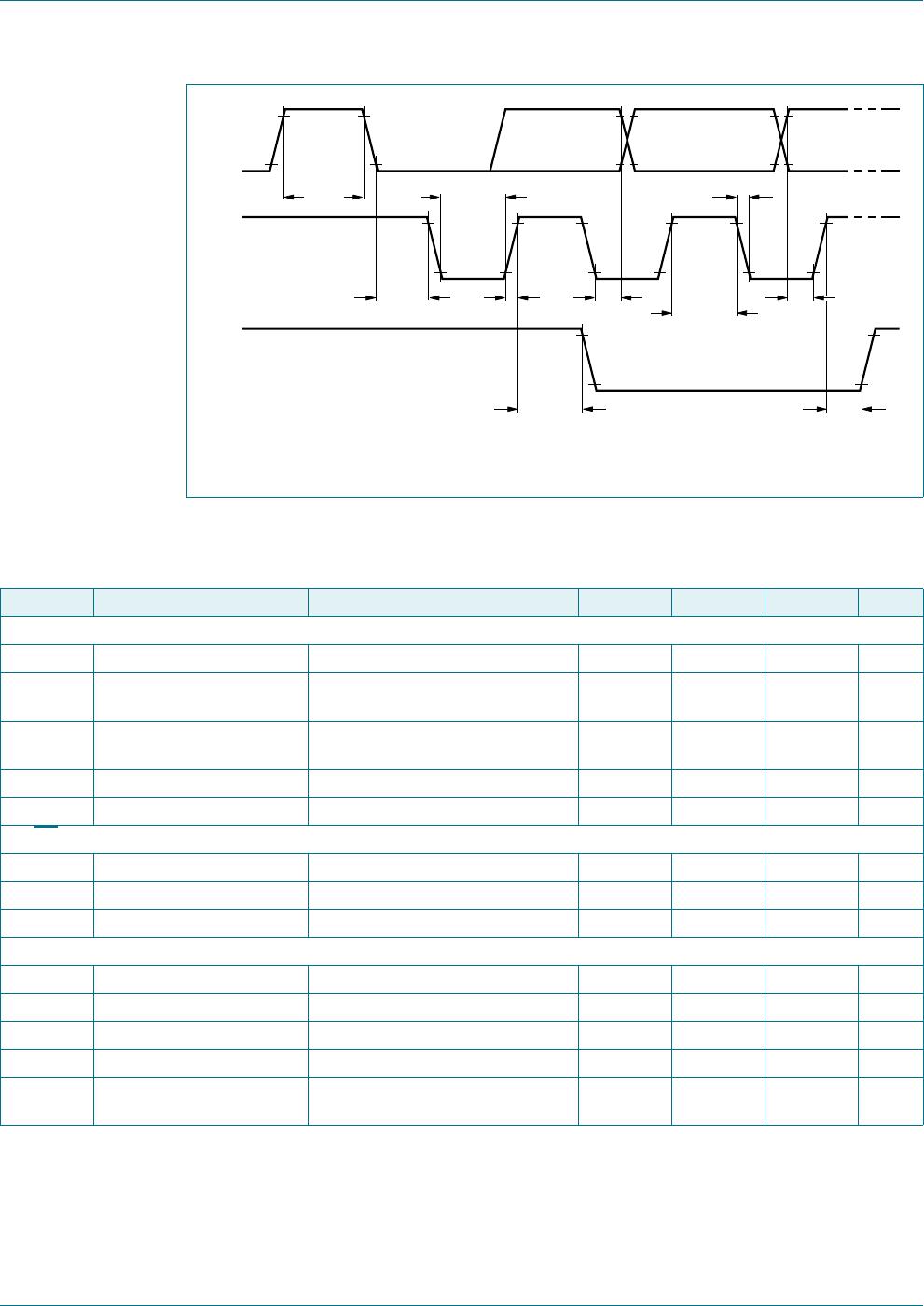
Fig 29. SPI-bus timing waveforms
DDD
&(
6&/
6',2
6',2
6$ 5$ E E E
6', E E E
E E E
6'2
5($'
:5,7(
KLJK=
5:
W
VX&(B1
W
UHF&(B1
W
U
W
I
W
+,*+
W
/2:
W
VX
W
G56',2
W
GLV6',2
W
W6',6'2
W
K
W
K&(B1