PCA8561 All information provided in this document is subject to legal disclaimers. © NXP Semiconductors N.V. 2015. All rights reserved.
Product data sheet Rev. 4 — 27 March 2015 25 of 55
NXP Semiconductors
PCA8561
Automotive 18 × 4 LCD segment driver
11. Bus interfaces
11.1 I
2
C-bus interface of the PCA8561A
The I
2
C-bus is for bidirectional, two-line communication between different ICs. The two
lines are a Serial DAta line (SDA) and a Serial CLock line (SCL). Both lines must be
connected to a positive supply via a pull-up resistor. Data transfer may be initiated only
when the bus is not busy. Both data and clock lines remain HIGH when the bus is not
busy. The PCA8561 acts as a slave receiver when being written to and as a slave
transmitter when being read from.
11.1.1 Bit transfer
One data bit is transferred during each clock pulse. The data on the SDA line must remain
stable during the HIGH period of the clock pulse, as changes in the data line at this time
are interpreted as STOP or START conditions.
Fig 18. I
2
C read and write protocol
DDD
:U
LWH
$&.IURP
VODYH
6 $
$ $
3
VODYHDGGUHVV ZULWHGDWD ZULWHGDWD ZULWHGDWD $
6
$
$
$
3
UHDGGDWD UHDGGDWD
UHDGGDWD
$
5H
DG
$&.IURP
VODYH
$&.IURP
VODYH
$&.IURP
PDVWHU
VODYHDGGUHVV
$&.IURP
VODYH
$&.IURP
VODYH
$&.IURP
PDVWHU
$&.IURP
VODYH
Fig 19. I
2
C read and write signaling
6
&/
6'
$
$&.
$&.
6
3
DDD
6
&/
6'
$
ELW ELW $&. $&.
6
67$57
FRQGLWLRQ
672
3
FRQGL
WLRQ
3
$&.RIVWE\WH
IURPVODYH
$&.RIQGE\WH
IURPVODYH
,
&
UHDGH[DPSOH
,
&ZULWHH[DPSOH
ELW ELW
VWE\WHVODYHDGGUHVVZLWK5: 
ZULWHQGE\WH
67$57
FRQGLWLRQ
672
3
FRQGL
WLRQ
VWE\WHVODYHDGGUHVVZLWK5: 
$&.RIVWE\WH
IURPVODYH
$&.RIQGE\WH
IURPVODYH
ELW ELW
ELW
ELW
UHDGQGE\WH
PCA8561 All information provided in this document is subject to legal disclaimers. © NXP Semiconductors N.V. 2015. All rights reserved.
Product data sheet Rev. 4 — 27 March 2015 26 of 55
NXP Semiconductors
PCA8561
Automotive 18 × 4 LCD segment driver
11.1.2 START and STOP conditions
A HIGH-to-LOW transition of the data line while the clock is HIGH is defined as the START
condition - S.
A LOW-to-HIGH transition of the data line while the clock is HIGH is defined as the STOP
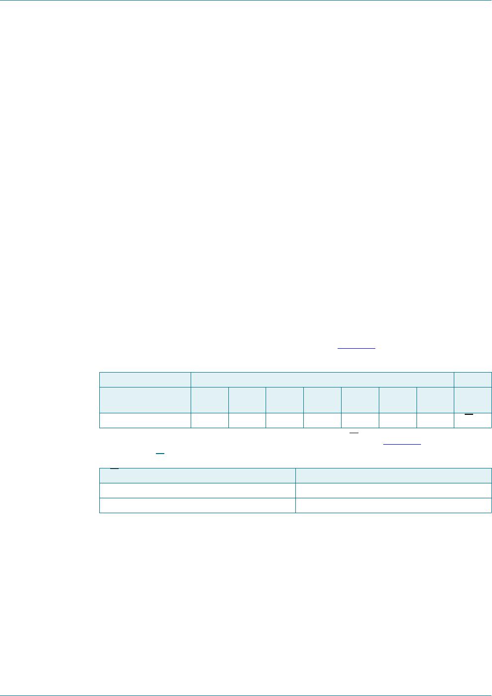
condition - P (see Figure 19
).
11.1.3 Acknowledge
Each byte of 8 bits is followed by an acknowledge cycle. An acknowledge is defined as
logic 0. A not-acknowledge is defined as logic 1.
When written to, the slave will generate an acknowledge after the reception of each byte.
After the acknowledge, another byte may be transmitted. It is also possible to send a
STOP or START condition.
When read from, the master receiver must generate an acknowledge after the reception
of each byte. When the master receiver no longer requires bytes to be transmitted, it must
generate a not-acknowledge. After the not-acknowledge, either a STOP or START
condition must be sent.
Remark: The PCA8561 omits the not-acknowledge. After the last byte read, the end of
transmission is indicated by a STOP or START condition from the master.
A detailed description of the I
2
C-bus specification is given in Ref. 12 “UM10204.
11.1.4 I
2
C interface protocol
The PCA8561 uses the I
2
C interface for data transfer. Interpretation of the data is
determined by the interface protocol.
11.1.4.1 Write protocol
After the I
2
C slave address is transmitted, the PCA8561 requires that the register address
pointer is defined. It can take the value 00h to 0Fh. Values outside of that range will result
in the transfer being ignored, however the slave will still respond with acknowledge
pulses.
After the register address has been transmitted, write data is transmitted. The minimum
number of data write bytes is 0 and the maximum number is unlimited. After each write,
the address pointer increments by one. After address 0Fh, the address pointer stops
incrementing at address 10h.
I
2
C START condition
I
2
C slave address + write
start register pointer
write data
write data
:
write data
I
2
C STOP condition; an I
2
C RE-START condition is also possible.
PCA8561 All information provided in this document is subject to legal disclaimers. © NXP Semiconductors N.V. 2015. All rights reserved.
Product data sheet Rev. 4 — 27 March 2015 27 of 55
NXP Semiconductors
PCA8561
Automotive 18 × 4 LCD segment driver
11.1.4.2 Read protocol
When reading the PCA8561, reading starts at the current position of the address pointer.
The address pointer for read data should first be defined by a write sequence.
I
2
C START condition
I
2
C slave address + write
start address pointer
I
2
C STOP condition; an I
2
C RE-START condition is also possible.
After setting the address pointer, a read can be executed. After the I
2
C slave address is
transmitted, the PCA8561 will immediately output read data. After each read, the address
pointer increments by one. After address 0Fh, the address pointer stops incrementing at
10h.
I
2
C START condition
I
2
C slave address + read
read data (master sends acknowledge bit)
:
11.1.4.3 I
2
C-bus slave address
Device selection depends on the I
2
C-bus slave address. Four different I
2
C-bus slave
addresses can be used to address the PCA8561 (see Table 13
).
The least significant bit of the slave address byte is bit R/W (see Table 14).
Bit 1 and bit 2 of the slave address are defined by connecting the input pins A0 and A1 to
either V
SS
(logic 0) or V
DD
(logic 1). Therefore, four instances of PCA8561 can be
distinguished on the same I
2
C-bus.
Table 13. I
2
C slave address byte
Slave address
Bit 7
MSB
6 5 4 3 2 1 0
LSB
01110A1A0R/W
Table 14. R/W-bit description
R/W Description
0 write data
1 read data

PCA8561BHN/AY

Mfr. #:
Manufacturer:
NXP Semiconductors
Description:
Equalizers Automotive 18 X 4 LCD segment driver
Lifecycle:
New from this manufacturer.
Delivery:
DHL FedEx Ups TNT EMS
Payment:
T/T Paypal Visa MoneyGram Western Union

Products related to this Datasheet