PCA8561 All information provided in this document is subject to legal disclaimers. © NXP Semiconductors N.V. 2015. All rights reserved.
Product data sheet Rev. 4 — 27 March 2015 13 of 55
NXP Semiconductors
PCA8561
Automotive 18 × 4 LCD segment driver
9. Possible display configurations
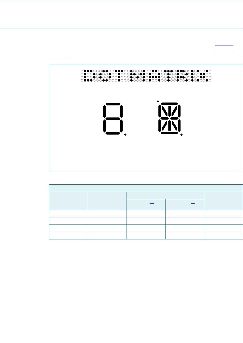
The possible display configurations of the PCA8561 depend on the number of active
backplane outputs required. A selection of display configurations is shown in Table 11
. All
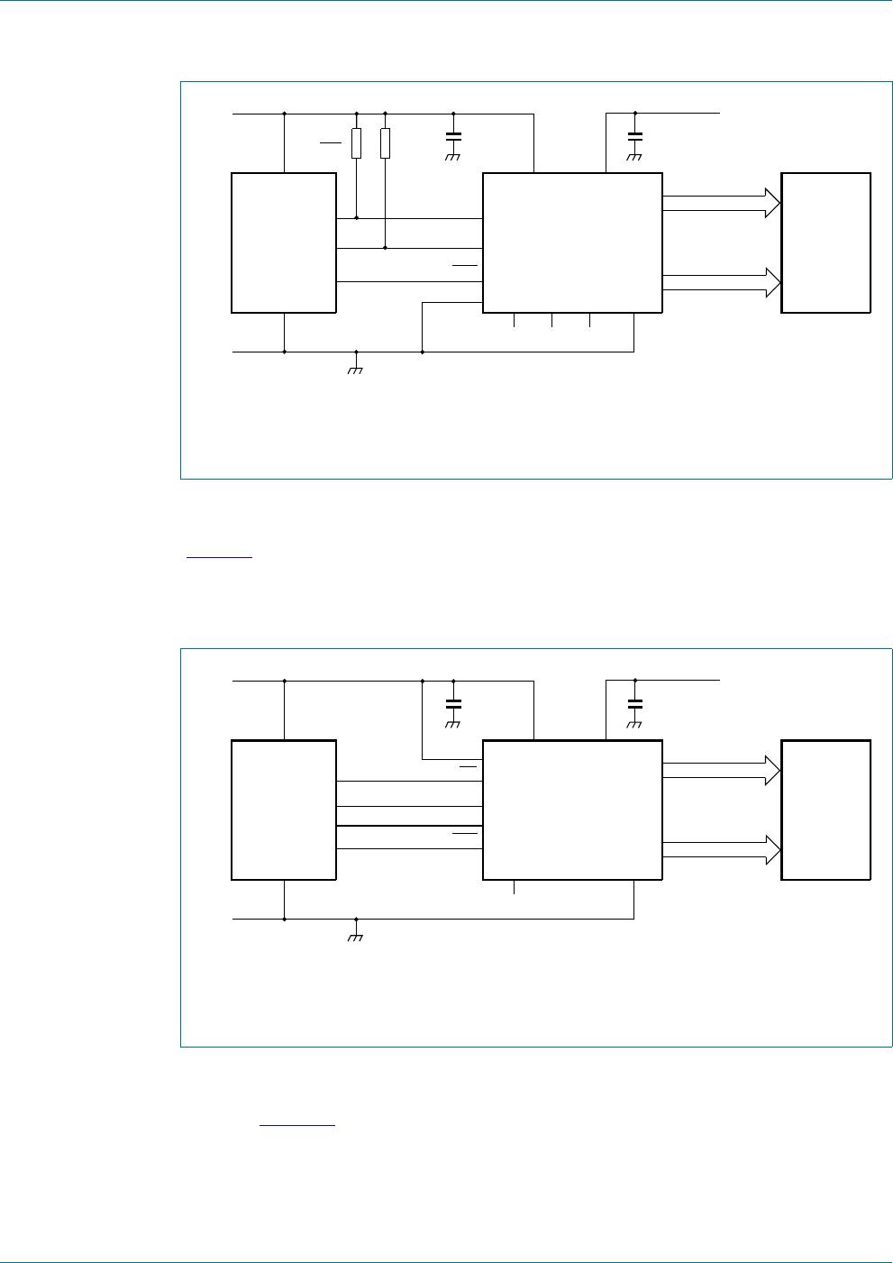
of these configurations can be implemented in the typical systems shown in Figure 9
or
Figure 10
.
[1] 7 segment display has 8 segments/elements including the decimal point.
[2] 14 segment display has 16 segments/elements including decimal point and accent dot.
Fig 8. Example of displays suitable for PCA8561
Table 11. Selection of possible display configurations
Number of
Backplanes Icons Digits/Characters Dot matrix:
segments/
elements
7-segment
[1]
14-segment
[2]
4729472 dots (4 18)
3546354 dots (3 18)
2364236 dots (2 18)
1182118dots (1 18)
VHJPHQWZLWKGRW VHJPHQWZLWKGRWDQGDFFHQW
DDD
GRWPDWUL[
PCA8561 All information provided in this document is subject to legal disclaimers. © NXP Semiconductors N.V. 2015. All rights reserved.
Product data sheet Rev. 4 — 27 March 2015 14 of 55
NXP Semiconductors
PCA8561
Automotive 18 × 4 LCD segment driver
The host microcontroller manages the 2-line I
2
C-bus communication channel with the
PCA8561. The internal oscillator is used and the internal POR is disabled in the example
(Figure 9
). The appropriate biasing voltages for the multiplexed LCD waveforms are
generated internally. The only other connections required to complete the system are the
reset, the power supplies (V
DD
, V
SS
, and V
LCD
) and the LCD panel chosen for the
application.
The host microcontroller manages the 3-line SPI-bus communication channel with the
PCA8561. The internal oscillator is enabled and the internal POR is enabled in the
example (Figure 10
). The appropriate biasing voltages for the multiplexed LCD
waveforms are generated internally. The only other connections required to complete the
system are reset, the power supplies (V
DD
, V
SS
, and V
LCD
) and the LCD panel chosen for
the application.
The resistance of the power lines must be kept to a minimum. A decoupling capacitor of at least
100 nF is recommended for the supplies.
Fig 9. Typical system configuration using I
2
C-bus, internal power-on reset disabled
The resistance of the power lines must be kept to a minimum. A decoupling capacitor of at least
100 nF is recommended for the supplies.
Fig 10. Typical system configuration using SPI-bus, internal power-on reset enabled
+267
0,&52
&21752//(5
5

W
U
&
E
6'$
6&/
VHJPHQWGULYHV
EDFNSODQHV
/&'3
$1(/
XSWR
HOHPHQWV
3&$$
9
''
9
66
966
DDD
9/&'
9
/&'
9''
&/.
QF QF QF
$$
325(
Q)
Q)
567
+267
0,&52
&21752//(5
6',2
6&/
VHJPHQWGULYHV
EDFNSODQHV
/&'3
$1(/
XSWR
HOHPHQWV
3&$%
9
''
9
66
966
DDD
9/&'
9
/&'
9''
&/.
QF
325(
Q)
Q)
&(
567
PCA8561 All information provided in this document is subject to legal disclaimers. © NXP Semiconductors N.V. 2015. All rights reserved.
Product data sheet Rev. 4 — 27 March 2015 15 of 55
NXP Semiconductors
PCA8561
Automotive 18 × 4 LCD segment driver
9.1 LCD bias generator
Fractional LCD biasing voltages are obtained from an internal voltage divider of three
impedances connected between V
LCD
and V
SS
. These intermediate levels are tapped off
at positions of
1
3
and
2
3
, or
1
2
, depending on the bias mode chosen. To keep current
consumption to a minimum, on-chip low-power buffers provide these levels to the display.
9.2 LCD voltage selector
The LCD voltage selector coordinates the multiplexing of the LCD in accordance with the
selected LCD drive configuration. The operation of the voltage selector is controlled by the
Display_ctrl_1 command (see Table 7
). The biasing configurations that apply to the
preferred modes of operation, together with the biasing characteristics as functions of
V
LCD
and the resulting discrimination ratios (D) are given in Table 12.
A practical value for V
LCD
is determined by equating V
off(RMS)
with a defined LCD
threshold voltage (V
th(off)
), typically when the LCD exhibits approximately 10 % contrast. In
the static drive mode, a suitable choice is V
LCD
>3V
th(off)
.
Multiplex drive modes of 1:3 and 1:4 with
1
2
bias are possible but the discrimination and
hence the contrast ratios are smaller.
Bias is calculated with Equation 2
(2)
The values for a
bias
are:
a
bias
= 1 for
1
2
bias
a
bias
= 2 for
1
3
bias
The RMS on-state voltage (V
on(RMS)
) for the LCD is calculated with Equation 3:
(3)
Table 12. Biasing characteristics
LCD drive
mode
Number of: LCD bias
configuration
Backplanes Levels
static 1 2 static 0 1
1:2 multiplex 2 3
1
2
0.354 0.791 2.236
1:2 multiplex 2 4
1
3
0.333 0.745 2.236
1:3 multiplex 3 4
1
3
0.333 0.638 1.915
1:4 multiplex 4 4
1
3
0.333 0.577 1.732
V
off RMS
V
LCD
-------------------------
V
on RMS
V
LCD
------------------------
D
V
on RMS
V
off RMS
-------------------------=
1
1a
bias
+
---------------------
V
on RMS
a
bias
2
2a
bias
n
MUX
++
n
MUX
1a
bias
+
2
-----------------------------------------------------
V
LCD
=
PCA8561BHN/AY

Mfr. #:
Manufacturer:
NXP Semiconductors
Description:
Equalizers Automotive 18 X 4 LCD segment driver
Lifecycle:
New from this manufacturer.
Delivery:
DHL FedEx Ups TNT EMS
Payment:
T/T Paypal Visa MoneyGram Western Union

Products related to this Datasheet