1.2 GHz Clock Distribution IC, 1.6 GHz Inputs,
Dividers, Five Outputs
Enhanced Product
AD9512-EP
Rev. 0
Information furnished by Analog Devices is believed to be accurate and reliable. However, no
responsibility is assumed by Analog Devices for its use, nor for any infringements of patents or other
rights of third parties that may result from its use. Specifications subject to change without notice. No
license is granted by implication or otherwise under any patent or patent rights of Analog Devices.
Trademarks and registered trademarks are the property of their respective owners.
One Technology Way, P.O. Box 9106, Norwood, MA 02062-9106, U.S.A.
Tel: 781.329.4700
www.analog.com
Fax: 781.461.3113 ©2012 Analog Devices, Inc. All rights reserved.
FEATURES
Two 1.6 GHz, differential clock inputs
5 programmable dividers, 1 to 32, all integers
3 independent 1.2 GHz LVPECL outputs
Additive output jitter 225 fs rms
2 independent 800 MHz/250 MHz LVDS/CMOS clock outputs
Additive output jitter: 275 fs rms
Serial control port
Space-saving 48-lead LFCSP
ENHANCED PRODUCT FEATURES
Supports defense and aerospace applications (AQEC
standard)
Military temperature range (−55°C to +85°C)
Controlled manufacturing baseline
1 assembly/test site
1 fabrication site
Enhanced product change notification
Qualification data available on request
APPLICATIONS
Low jitter, low phase noise clock distribution
Clocking high speed ADCs, DACs, DDSs, DDCs, DUCs, MxFEs
Defense and aerospace applications
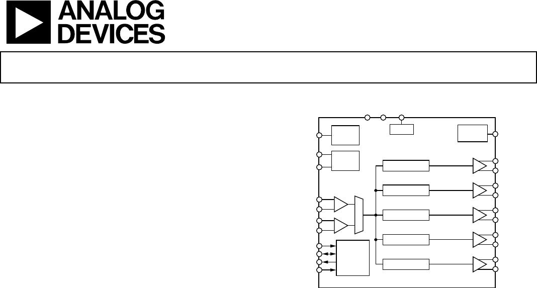
FUNCTIONAL BLOCK DIAGRAM
Figure 1.
GENERAL DESCRIPTION
The AD9512-EP provides a multi-output clock distribution
in a design that emphasizes low jitter and low phase noise to
maximize data converter performance. Other applications
with demanding phase noise and jitter requirements can also
benefit from this part.
There are five independent clock outputs. Three outputs are
LVPECL (1.2 GHz), and two are selectable as either LVDS
(800 MHz) or CMOS (250 MHz) levels.
Each output has a programmable divider that can be bypassed
or set to divide by any integer up to 32. The phase of one clock
output relative to another clock output can be varied by means
of a divider phase select function that serves as a coarse timing
adjustment.
The AD9512-EP is ideally suited for data converter clocking
applications where maximum converter performance is
achieved by encode signals with subpicosecond jitter.
The AD9512-EP is available in a 48-lead LFCSP and can be
operated from a single 3.3 V supply. The temperature range is
−55°C to +85°C.
Additional application and technical information can be found
in the AD9512 data sheet.
Note that the delay block element that exists in Channel 4 of the
AD9512 standard product is not supported in this AD9512-EP
version.
SYNC
STATUS
SYNC
STATUS
SCLK
SDIO
SDO
CSB
SERIAL
CONTROL
PORT
FUNCTION
SYNCB,
RESETB
PDB
DSYNC
DSYNCB
DETECT
SYNC
VREF
RSET
AD9512-EP
GNDVS
CLK1
CLK1B
CLK2
CLK2B
PROGRAMMABLE
DIVIDERS AND
PHASE ADJUST
OUT0
OUT0B
LVPECL
/1, /2, /3... /31, /32
OUT1
OUT1B
LVPECL
/1, /2, /3... /31, /32
OUT2
OUT2B
LVPECL
/1, /2, /3... /31, /32
OUT3
OUT3B
LVDS/CMOS
/1, /2, /3... /31, /32
OUT4
OUT4B
LVDS/CMOS
/1, /2, /3... /31, /32
10463-001
AD9512-EP Enhanced Product
Rev. 0 | Page 2 of 20
TABLE OF CONTENTS
Features .............................................................................................. 1
Enhanced Product Features ............................................................ 1
Applications ....................................................................................... 1
Functional Block Diagram .............................................................. 1
General Description ......................................................................... 1
Revision History ............................................................................... 2
Specifications ..................................................................................... 3
Clock Inputs .................................................................................. 3
Clock Outputs ............................................................................... 3
Timing Characteristics ................................................................ 4
Clock Output Phase Noise .......................................................... 5
Clock Output Additive Time Jitter ............................................. 8
Serial Control Port ..................................................................... 10
FUNCTION Pin ......................................................................... 10
SYNC STATUS Pin .................................................................... 11
Power............................................................................................ 11
Absolute Maximum Ratings ......................................................... 12
Thermal Characteristics ............................................................ 12
Pin Configuration and Function Descriptions ........................... 13
Typical Performance Characteristics ........................................... 15
Outline Dimensions ....................................................................... 18
Ordering Guide .......................................................................... 18
REVISION HISTORY
3/12Revision 0: Initial Version
Enhanced Product AD9512-EP
Rev. 0 | Page 3 of 20
SPECIFICATIONS
Typical (Typ) is given for V
S
= 3.3 V ± 5%; T
A
= 25°C, R
SET
= 4.12 kΩ, unless otherwise noted. Minimum (Min) and Maximum (Max)
values are given over full V
S
and T
A
(−55°C to +85°C) variation.
CLOCK INPUTS
Table 1.
Parameter Min Typ Max Unit Test Conditions/Comments
CLOCK INPUTS (CLK1, CLK2)
1
Input Frequency 0 1.6 GHz
Input Sensitivity 150
2
mV p-p Jitter performance can be improved with higher slew
rates (greater swing).
Input Level 2
3
V p-p Larger swings turn on the protection diodes and can
degrade jitter performance.
Input Common-Mode Voltage, V
CM
1.45 1.6 1.7 V Self-biased; enables ac coupling; at full temperature range
1.5 1.6 1.7 V At −40°C to +85°C.
Input Common-Mode Range, V
CMR
1.3 1.8 V With 200 mV p-p signal applied; dc-coupled.
Input Sensitivity, Single-Ended 150 mV p-p CLK2 ac-coupled; CLK2B ac bypassed to RF ground.
Input Resistance 4.0 4.8 5.6 Self-biased.
Input Capacitance 2 pF
1
CLK1 and CLK2 are electrically identical; each can be used as either differential or single-ended input.
2
With a 50 Ω termination, this is −12.5 dBm.
3
With a 50 Ω termination, this is +10 dBm.
CLOCK OUTPUTS
Table 2.
Parameter Min Typ Max Unit Test Conditions/Comments
LVPECL CLOCK OUTPUTS Termination = 50 Ω to V
S
2 V
OUT0, OUT1, OUT2; Differential Output level 0x3D (0x3E) (0x3F)[3:2] = 10b
Output Frequency 1200 MHz See Figure 10
Output High Voltage (V
OH
) V
S
− 1.22 V
S
− 0.98 V
S
− 0.93 V
Output Low Voltage (V
OL
) V
S
− 2.10 V
S
− 1.80 V
S
− 1.67 V
Output Differential Voltage (V
OD
) 660 810 965 mV
LVDS CLOCK OUTPUTS
Termination = 100 Ω differential; default
OUT3, OUT4; Differential Output level 0x40 (0x41)[2:1] = 01b
3.5 mA termination current
Output Frequency 800 MHz See Figure 11
Differential Output Voltage (V
OD
) 250 360 450 mV
Delta V
OD
25 mV
Output Offset Voltage (V
OS
) 1.05 1.23 1.375 V At full temperature range
1.125 1.23 1.375 V At −40°C to +85°C
Delta V
OS
25 mV
Short-Circuit Current (I
SA
, I
SB
) 14 24 mA Output shorted to GND
CMOS CLOCK OUTPUTS
OUT3, OUT4 Single-ended measurements;
B outputs: inverted, termination open
Output Frequency 250 MHz With 5 pF load each output; see Figure 12
Output Voltage High (V
OH
) V
S
− 0.1 V @ 1 mA load
Output Voltage Low (V
OL
) 0.1 V @ 1 mA load

AD9512UCPZ-EP

Mfr. #:
Manufacturer:
Analog Devices Inc.
Description:
Clock Drivers & Distribution 1.2GHz Dividers Delay Adj 5 Outputs
Lifecycle:
New from this manufacturer.
Delivery:
DHL FedEx Ups TNT EMS
Payment:
T/T Paypal Visa MoneyGram Western Union

Products related to this Datasheet