Enhanced Product AD9512-EP
Rev. 0 | Page 13 of 20
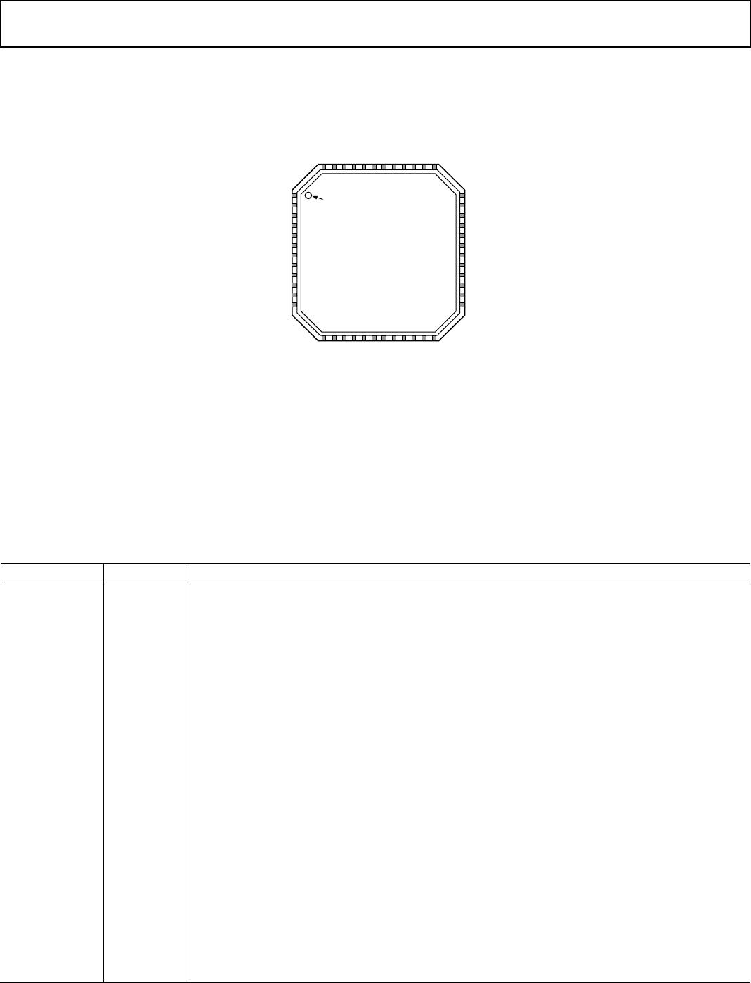
PIN CONFIGURATION AND FUNCTION DESCRIPTIONS
Figure 2. Pin Configuration
Table 12. Pin Function Descriptions
Pin No. Mnemonic Description
Detect Sync. Used for multichip synchronization.
2 DSYNCB Detect Sync Complement. Used for multichip synchronization.
3, 4, 6, 9, 18,
22, 23, 25, 28,
29, 32, 33, 36,
39, 40, 44, 47, 48
VS Power Supply (3.3 V).
5 DNC Do Not Connect. Do not connect to this pin.
7 CLK2 Clock Input.
8 CLK2B Complementary Clock Input. Used in conjunction with CLK2.
10 CLK1 Clock Input.
11 CLK1B Complementary Clock Input. Used in conjunction with CLK1.
Multipurpose Input. Can be programmed as a reset (RESETB), sync (SYNCB), or power-down (PDB) pin.
13 SYNC STATUS Output Used to Monitor the Status of Multichip Synchronization.
14 SCLK Serial Data Clock.
15 SDIO Serial Data I/O.
16 SDO Serial Data Output.
17 CSB Serial Port Chip Select.
19, 24, 37,
38, 43, 46
GND Ground.
20 OUT2B Complementary LVPECL Output.
21 OUT2 LVPECL Output.
26 OUT1B Complementary LVPECL Output.
30 OUT4B Complementary LVDS/Inverted CMOS Output.
NOTES
1. DNC = DO NOT CONNECT TO THIS PIN.
2. THE EXPOSED PADDLE ON THIS PACKAGE IS AN ELECTRICAL
CONNECTION AS WELL AS A THERMAL ENHANCEMENT. FOR
THE DEVICE TO FUNCTION PROPERLY, THE PADDLE MUST BE
ATTACHED TO GROUND, GND.
PIN 1
INDICATOR
48
47
46
45
44
43
42
41
40
39
38
VS
VS
GND
RSET
VS
GND
OUT0
OUT0B
VS
VS
GND
1
2
3
4
5
6
7
8
9
10
11
12
DSYNC
DSYNCB
VS
VS
DNC
VS
CLK2
CLK2B
VS
CLK1
CLK1B
FUNCTION
VS
OUT3
OUT3B
VS
VS
OUT4
OUT4B
VS
VS
OUT1
OUT1B
VS
36
35
34
33
32
31
30
29
28
27
26
25
13
14
15
16
17
18
19
20
21
22
23
24
SYNC STATUS
SCLK
SDIO
SDO
CSB
VS
GND
OUT2B
OUT2
VS
VS
GND
37 GND
AD9512-EP
TOP VIEW
(Not to Scale)
10463-002