IDT 89HPES24NT24G2 Datasheet
17 of 35 December 17, 2013
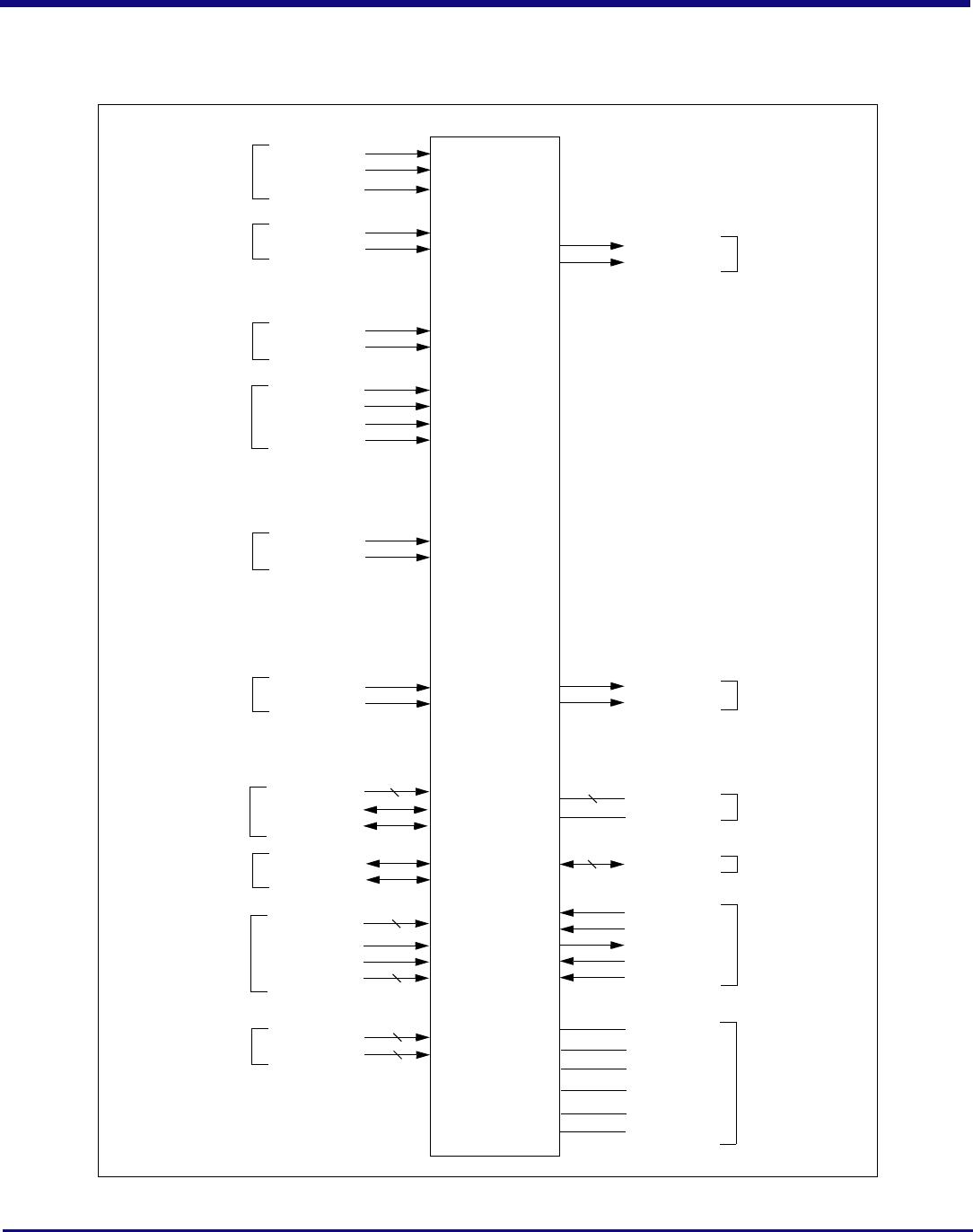
System Clock Parameters
Values based on systems running at recommended supply voltages and operating temperatures, as shown in Tables 16 and 15.
Note: Refclk jitter compliant to PCIe Gen2 Common Clock architecture is adequate for the GCLKN/P[x] and PE[x]CLKN/P pins of this IDT
PCIe switch. This same jitter specification is applicable when interfacing the switch to another IDT switch in a Separate (Non-Common)
Clock architecture.
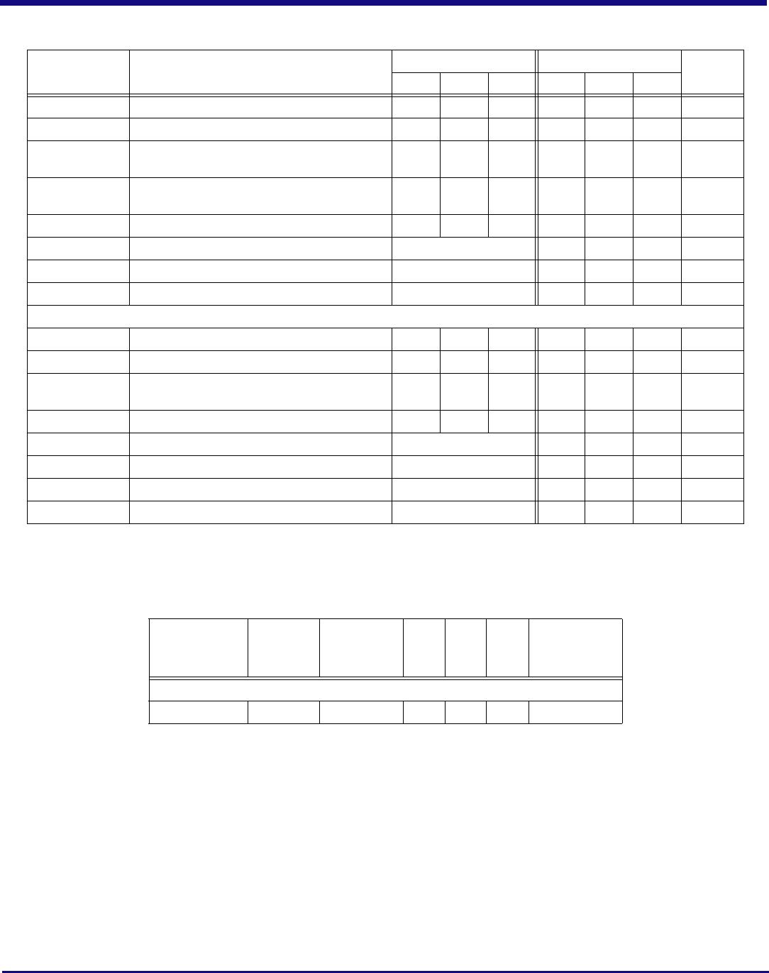
AC Timing Characteristics
Parameter Description Condition Min Typical Max Unit
Refclk
FREQ
Input reference clock frequency range 100 125
1
1.
The input clock frequency will be either 100 or 125 MHz depending on signal GCLKFSEL.
MHz
T
C-RISE
Rising edge rate Differential 0.6 4 V/ns
T
C-FALL
Falling edge rate Differential 0.6 4 V/ns
V
IH
Differential input high voltage Differential +150 mV
V
IL
Differential input low voltage Differential -150 mV
V
CROSS
Absolute single-ended crossing point
voltage
Single-ended +250 +550 mV
V
CROSS-DELTA
Variation of V
CROSS
over all rising clock
edges
Single-ended +140 mV
V
RB
Ring back voltage margin Differential -100 +100 mV
T
STABLE
Time before V
RB
is allowed Differential 500 ps
T
PERIOD-AVG
Average clock period accuracy -300 2800 ppm
T
PERIOD-ABS
Absolute period, including spread-spec-
trum and jitter
9.847 10.203 ns
T
CC-JITTER
Cycle to cycle jitter 150 ps
V
MAX
Absolute maximum input voltage +1.15 V
V
MIN
Absolute minimum input voltage -0.3 V
Duty Cycle Duty cycle 40 60 %
Rise/Fall Matching Single ended rising Refclk edge rate ver-
sus falling Refclk edge rate
20 %
Z
C-DC
Clock source output DC impedance 40 60
Table 11 Input Clock Requirements
Parameter Description
Gen 1 Gen 2
Units
Min
1
Typ
1
Max
1
Min
1
Typ
1
Max
1
PCIe Transmit
UI Unit Interval 399.88 400 400.12 199.94 200 200.06 ps
T
TX-EYE
Minimum Tx Eye Width 0.75 0.75 UI
T
TX-EYE-MEDIAN-to-
MAX-JITTER
Maximum time between the jitter median and maxi-
mum deviation from the median
0.125 UI
Table 12 PCIe AC Timing Characteristics (Part 1 of 2)