IDT 89HPES24NT24G2 Datasheet
21 of 35 December 17, 2013
Recommended Operating Supply Voltages — Industrial Temperature
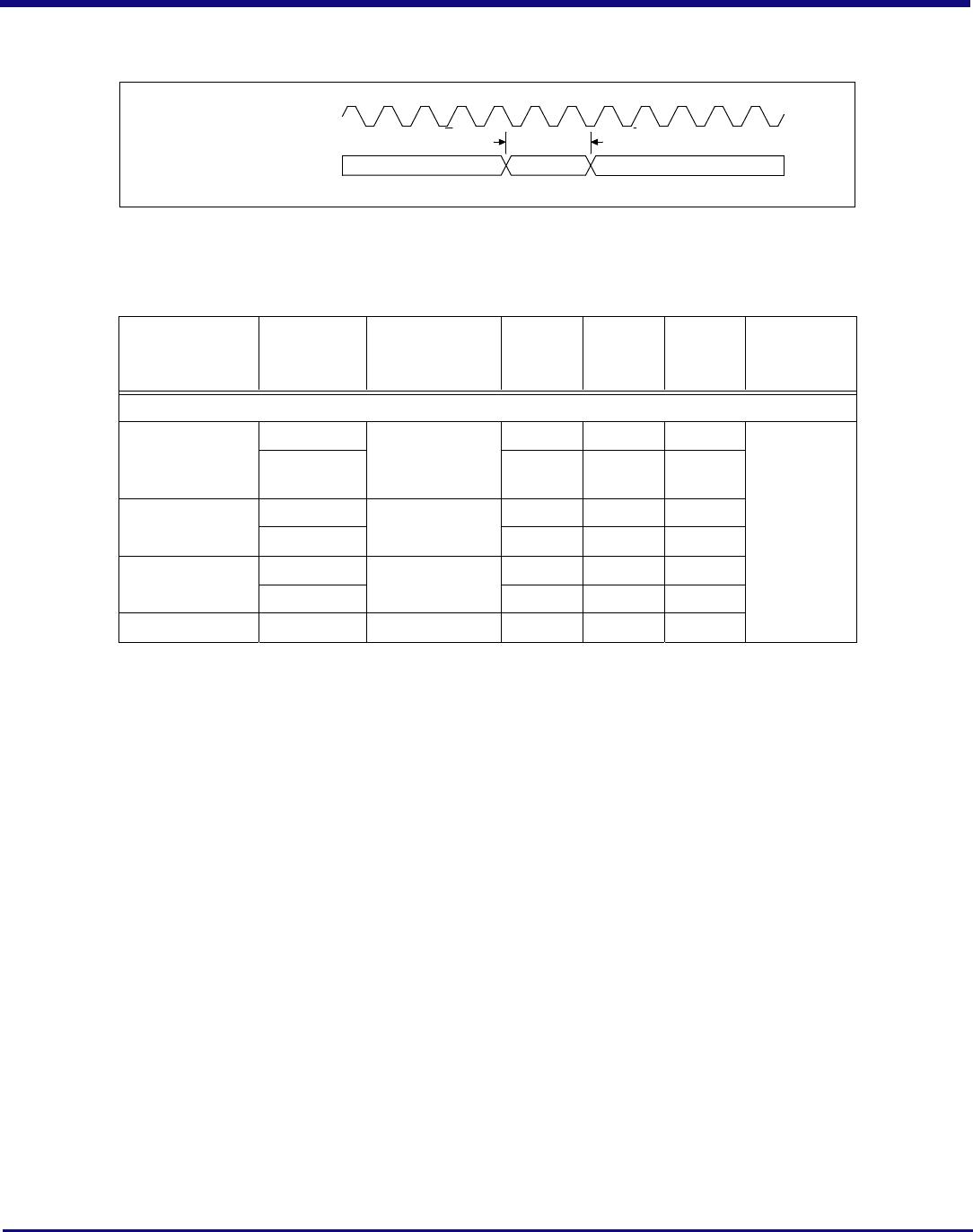
Power-Up/Power-Down Sequence
During power supply ramp-up, V
DD
CORE must remain at least 1.0V below V
DD
I/O at all times. There are no other power-up sequence require-
ments for the various operating supply voltages.
The power-down sequence can occur in any order.
Power Consumption
Typical power is measured under the following conditions: 25°C Ambient, 35% total link usage on all ports, typical voltages defined in Table 16
(and also listed below).
Maximum power is measured under the following conditions: 70°C Ambient, 85% total link usage on all ports, maximum voltages defined in
Table 16 (and also listed below).
Note 1: The above power consumption assumes that all ports are functioning at Gen2 (5.0 GT/S) speeds. Power consumption can be
reduced by turning off unused ports through software or through boot EEPROM. Power savings will occur in V
DD
PEA, V
DD
PEHA, and
V
DD
PETA. Power savings can be estimated as directly proportional to the number of unused ports, since the power consumption of a turned-
off port is close to zero. For example, if 3 ports out of 16 are turned off, then the power savings for each of the above three power rails can be
calculated quite simply as 3/16 multiplied by the power consumption indicated in the above table.
Note 2: Using a port in Gen1 mode (2.5GT/S) results in approximately 18% power savings for each power rail: V
DD
PEA, V
DD
PEHA, and
V
DD
PETA.
Symbol Parameter Minimum Typical Maximum Unit
V
DD
CORE Internal logic supply 0.9 1.0 1.1 V
V
DD
I/O I/O supply except for SerDes 3.125 3.3 3.465 V
V
DD
PEA
1
1.
V
DD
PEA and V
DD
PETA should have no more than 25mV
peak-peak
AC power supply noise superimposed on the 1.0V nominal DC
value.
PCI Express Analog Power 0.95 1.0 1.05 V
V
DD
PEHA
2
2.
V
DD
PEHA should have no more than 50mV
peak-peak
AC power supply noise superimposed on the 2.5V nominal DC value.
PCI Express Analog High Power 2.25 2.5 2.75 V
V
DD
PETA
1
PCI Express Transmitter Analog Voltage 0.95 1.0 1.1 V
V
SS
Common ground 0 0 0 V
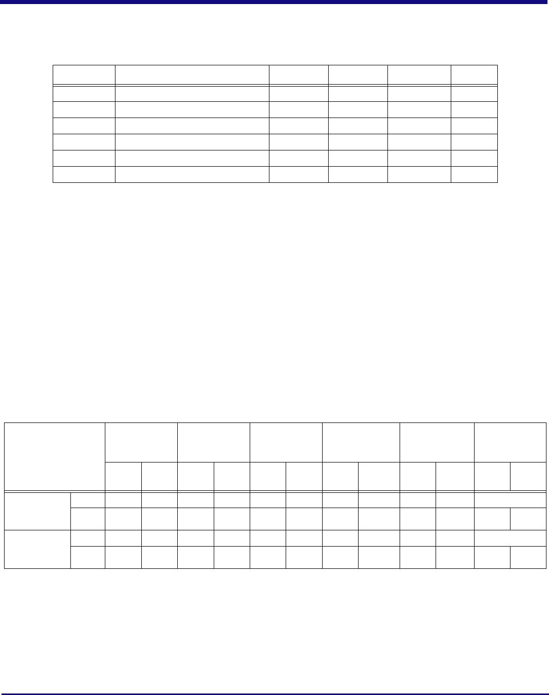
Table 17 PES24NT24G2 Operating Voltages — Industrial Temperature
Number of Active
Lanes per Port
Core Supply
PCIe Analog
Supply
PCIe Analog
High Supply
PCIe
Transmitter
Supply
I/O Supply Total
Typ
1.0V
Max
1.1V
Typ
1.0V
Max
1.1V
Typ
2.5V
Max
2.75V
Typ
1.0V
Max
1.1V
Typ
3.3V
Max
3.465
Typ
Power
Max
Power
x8/x8/x1/x1/x1/
x1/x1/x1/x1/x1/
(Full Swing)
mA 2540 3400 1384 1570 184 205 578 699 3 5
Watts 2.54 3.74 1.38 1.73 0.46 0.56 0.58 0.77 0.01 0.02 4.97 6.82
x8/x8/x1/x1/x1/
x1/x1/x1/x1/x1/
(Half Swing)
mA 2540 3400 1190 1350 184 205 301 364 3 5
Watts 2.54 3.74 1.19 1.49 0.46 0.56 0.30 0.40 0.01 .02 4.50 6.21
Table 18 PES24NT24G2 Power Consumption