LTC5569
10
5569fb
For more information www.linear.com/LTC5569
TEST CIRCUIT
LO
IN
50Ω
1516
1
2
3
14 13
65
4
12
11
10
9
7 8
C6
IFA
OUT
190MHz
50Ω
RFA
IN
50Ω
L1
L5
BIASA
RF
0.015"
0.062"
0.015"
GND
BIAS
GND
RFA
GND
C1
DC1719A
EVALUATION BOARD
LAYER STACK-UP
(NELCO N4000-13)
C3
GND
RFB
BIASB IFB
+
IFB
ENB
GND
LO
ENA
ENA
C11
V
CC
3.3V
ENB
V
CCB
IFA
+
17
GND
IFA
V
CCA
T1
8:1
LTC5569
T2
8:1
L3
L2 L4
C9
IFB
OUT
190MHz
50Ω
C8
C5
RFB
IN
50Ω
L6
C2
C4
C10
5569 F01
C7
APPLICATION RF MATCH LO MATCH
RF (MHz) LO C1, C2 C3, C4 L5, L6 C5 C6
300 to 400 HS 120pF 18pF 3.3nH 1nF 10pF
400 to 500 HS 120pF 12pF 2nH 27pF 6.8pF
700 to 1000 HS 68pF 4.7pF 6.8pF 2.2pF
1400 to 3000 LS, HS 2.7pF 3.9pF
3000 to 4000 LS 3.9pF 0.7pF 3.9pF 0.3pF
LS = Low side, HS = High side
REF DES VALUE SIZE VENDOR REF DES VALUE SIZE VENDOR
C1, C2 See Table 0402 AVX C11 2.2µF 0603 AVX
C3, C4 See Table 0402 AVX T1, T2 8:1 Mini-Circuits TC8-1-10LN+
C5 See Table 0402 AVX L1- L4 180nH 0603 Coilcraft 0603HP
C6 See Table 0402 AVX L5, L6 See Table 0402 Coilcraft 0402HP
C7-C10 10nF 0402 AVX
Figure 1. Standard Downmixer Test Circuit Schematic (190MHz Bandpass IF Matching)
LTC5569
11
5569fb
For more information www.linear.com/LTC5569
APPLICATIONS INFORMATION
Introduction
The LTC5569 incorporates two identical, symmetric double-
balanced active mixers with a common LO input, separate
RF inputs and separate IF outputs. See the Pin Functions
and Block Diagram sections for a description of each pin.
A test circuit schematic showing all external components
required for the data sheet specified performance is shown
in Figure 1. A few additional components may be used
to modify the DC supply current or frequency response,
which will be discussed in the following sections.
The LO and RF inputs are single ended. The IF outputs
are differential. Low side or high side LO injection may be
used. The test circuit, shown in Figure 1, utilizes bandpass
IF output matching and 8:1 IF transformers to realize 50Ω
single-ended IF outputs. The evaluation board layout is
shown in Figure 2.
RF Inputs
A simplified schematic of the A-channel mixers RF input
is shown in Figure 3. The B-channel is identical, and not
shown for clarity. As shown, one terminal of the integrated
RF transformers primary winding is connected to Pin 1,
while the other terminal is DC-grounded internally. For this
reason, a series DC-blocking capacitor (C1) is needed if the
RF source has DC voltage present. The DC resistance of
the primary winding is approximately 4Ω. The secondary
winding of the RF transformer is internally connected to
the RF buffer amplifier.
The RF inputs are 50Ω matched from 1400MHz to 3300MHz
with a single 2.7pF series capacitor on each input. Matching
to RF frequencies above or below this frequency range is
easily accomplished by adding shunt capacitor C3, shown
in Figure 3. For RF frequencies below 500MHz, series
Figure 2. Evaluation Board Layout
LTC5569
12
5569fb
For more information www.linear.com/LTC5569
APPLICATIONS INFORMATION
inductor L5 is also needed. The evaluation board does
not include pads for the series inductors, so the 50Ω RF
input traces need to be cut to install these in series. The
RF input matching element values for each application are
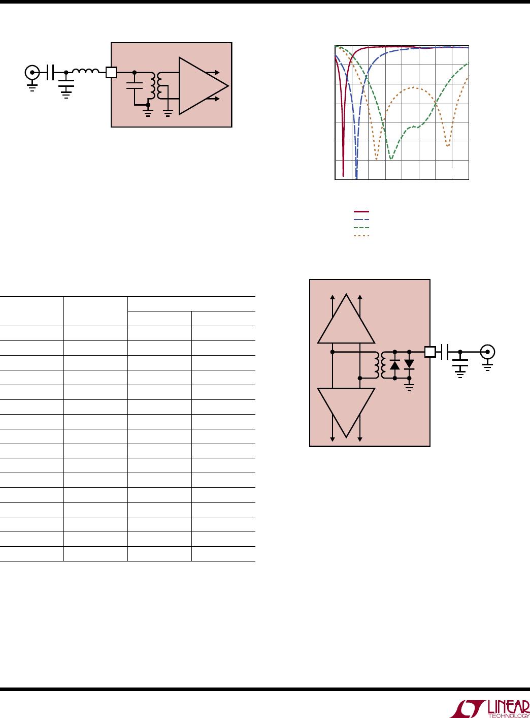
tabulated in Figure 1. Measured RF input return losses
are shown in Figure 4. The RF input impedance and input
reflection coefficient, versus frequency are listed in Table 1.
Table 1. RF Input Impedance and S11 (At Pin 1, No External
Matching, Mixer Enabled)
FREQUENCY
(MHz)
INPUT
IMPEDANCE
S11
MAG ANGLE
350 9.0 + j11.9 0.71 152.5
450 11.0 + j13.8 0.66 147.7
575 13.1 + j15.7 0.62 143.0
700 15.2 + j17.3 0.58 138.6
900 18.1 + j20.0 0.53 131.6
1100 21.3 + j22.4 0.49 124.6
1400 27.0 + j25.3 0.42 114.1
1700 33.4 + j26.8 0.36 103.9
1950 39.1 + j25.6 0.30 97.1
2200 43.4 + j21.5 0.23 94.2
2450 44.3 + j15.9 0.18 100.2
2700 40.8 + j9.9 0.15 126.5
3000 33.1 + j6.4 0.22 154.7
3300 24.3 + j6.8 0.36 159.9
3600 17.6 + j9.6 0.49 155.4
3900 12.9 + j12.7 0.61 149.6
LO Input
A simplified schematic of the LO input, with external
components is shown in Figure 5. Similar to the RF in
-
puts, the integrated LO transformers primary winding is
DC-grounded internally, and therefore requires an external
DC-blocking capacitor. Capacitor C5 provides the necessary
DC-blocking, and optimizes the LO input match over the
1GHz to 3.5GHz frequency range. The nominal LO input
level is 0dBm although the limiting amplifiers will deliver
excellent performance over a ±5dB input power range. LO
input power greater than +6dBm may cause conduction
of the internal ESD diodes.
To optimize the LO input match for frequencies below
1GHz, the value of C5 is increased and shunt capacitor C6
is added. A summary of values for C5 and C6, versus LO
frequency range is listed in Table 2. Measured LO input
LO
BUFFER
LO
BUFFER
LO
C6
5569 F05
LTC5569
11
C5
LO
IN
Figure 5. LO Input Schematic
RF
BUFFER
RFA
C3
5569 F03
L5
LTC5569
1
C1
RFA
IN
Figure 3. RF Input Schematic
Figure 4. RF Input Return Loss
FREQUENCY (GHz)
0.2
RETURN LOSS (dB)
–15
–10
–5
3.2
5569 F04
–20
–25
1.2 2.2
0.7 3.7
1.7 2.7
4.2
–30
–35
0
400MHz TO 500MHz APP.
700MHz TO 1000MHz APP.
1400MHz TO 3000MHz APP.
3GHz TO 4GHz APP.
T
C
= 25°C

LTC5569IUF#PBF

Mfr. #:
Manufacturer:
Analog Devices Inc.
Description:
RF Mixer 300MHz - 4GHz Dual Active Downconverting Mixer
Lifecycle:
New from this manufacturer.
Delivery:
DHL FedEx Ups TNT EMS
Payment:
T/T Paypal Visa MoneyGram Western Union

Products related to this Datasheet