LTC5569
4
5569fb
For more information www.linear.com/LTC5569
Note 1: Stresses beyond those listed under Absolute Maximum Ratings
may cause permanent damage to the device. Exposure to any Absolute
Maximum Rating condition for extended periods may affect device
reliability and lifetime.
Note 2: The LTC5569 is guaranteed functional over the –40°C to 105°C
case temperature range (θ
JC
= 8°C/W).
Note 3: SSB Noise Figure measured with a small-signal noise source,
bandpass filter and 2dB matching pad on RF input, and bandpass filter on
the LO input.
Note 4: Channel A to channel B isolation is measured as the relative IF
output power of channel B to channel A, with the RF input signal applied to
channel A. The RF input of channel B is 50Ω terminated, and both mixers
are enabled.
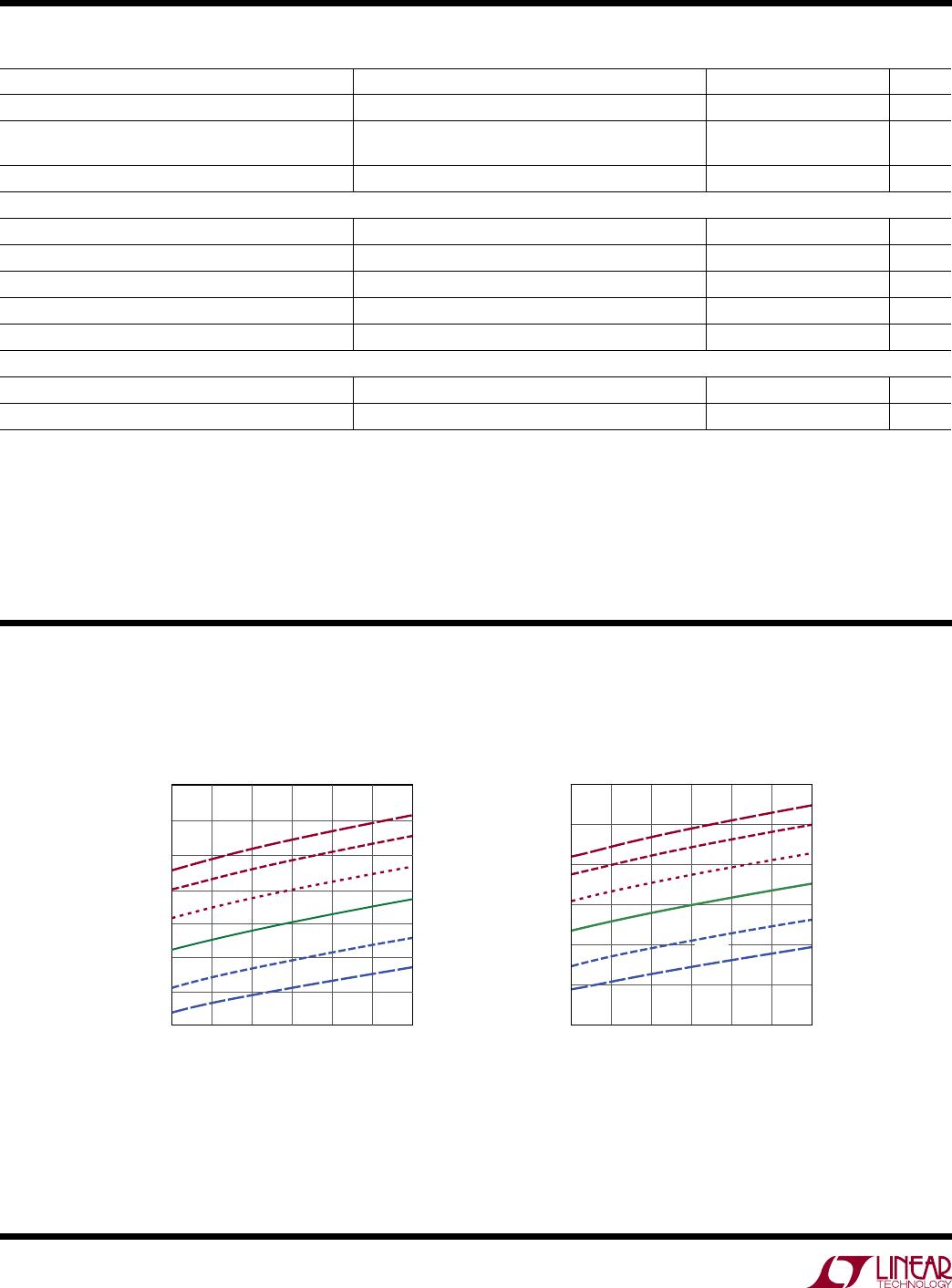
TYPICAL DC PERFORMANCE CHARACTERISTICS
Supply Current vs Supply Voltage
(One Mixer Enabled)
Supply Current vs Supply Voltage
(Both Mixers Enabled)
Test circuit shown in Figure 1.
DC ELECTRICAL CHARACTERISTICS
V
CC
= 3.3V, T
C
= 25°C. Test circuit shown in Figure 1. (Note 2)
PARAMETER CONDITIONS MIN TYP MAX UNITS
Supply Voltage (V
CC
) 3.0 3.3 3.6 V
Supply Current One Mixer Enabled
Both Mixers Enabled
ENA or ENB = High
ENA and ENB = High
90
180
106
212
mA
mA
Shutdown Current—Both Mixers Disabled ENA and ENB = Low 200 µA
Enable Logic Inputs (ENA, ENB)
ENA, ENB Input High Voltage (On) 2.5 V
ENA, ENB Input Low V
oltage (Off) 0.3 V
ENA, ENB Input Current –0.3V to V
CC
+ 0.3V 100 µA
Turn-On Time 0.6 µs
Turn-Off Time 0.5 µs
Mixer DC Bias Adjust (BIASA, BIASB)
Open-Circuit DC Voltage 2.2 V
Short-Circuit DC Current Pin Shorted to Ground 1.8 mA
V
CC
SUPPLY VOLTAGE (V)
3.0
T
C
= 105°C
85°C
55°C
25°C
–10°C
–40°C
96
94
92
90
88
86
84
3.3 3.5
3.1 3.2
3.4
V
CC
SUPPLY VOLTAGE (V)
3.0
165
SUPPLY CURRENT (mA)
170
175
180
185
T
C
= 105°C
85°C
55°C
25°C
–40°C
3.1
3.2 3.3 3.4
3.5
190
–10°C

