LTC5569
13
5569fb
For more information www.linear.com/LTC5569
APPLICATIONS INFORMATION
return losses are shown in Figure 6. Finally, LO input im-
pedance and input reflection coefficient, versus frequency
is shown in Table 3.
Table 2. LO Input Matching Values vs LO Frequency Range
FREQUENCY (MHz) C5 (pF) C6 (pF)
350 to 430 390 22
480 to 630 68 12
576 to 722 27 6.8
720 to 980 15 4.7
814 to 1155 6.8 2.2
1000 to 3500 3.9
2200 to 4000 3.9 0.3
The LO buffers have been designed such that the LO input
Figure 6. LO Input Return Loss
Figure 7. LO Input Return Loss for Three Operating States
FREQUENCY (GHz)
0.2
RETURN LOSS (dB)
–10
–5
0
1.7 2.7 4.2
5569 F06
–15
–20
–25
0.7 1.2
2.2
3.2 3.7
C5 = 27pF, C6 = 6.8pF
C5 = 6.8pF, C6 = 2.2pF
C5 = 3.9pF
C5 = 3.9pF, C6 = 0.3pF
T
C
= 25°C
FREQUENCY (GHz)
0.2
RETURN LOSS (dB)
0
–2
–4
–6
–8
–10
12
14
16
18
–20
4.2
5569 F07
1.2 2.2 3.2 3.70.7 1.7 2.7
T
C
= 25°C
C5 = 3.9pF
BOTH MIXERS DISABLED
ONE MIXER ENABLED
BOTH MIXERS ENABLED
Table 3. LO Input Impedance and S11 (At Pin 11, No External
Matching, Both Mixers Enabled)
FREQUENCY
(MHz)
INPUT
IMPEDANCE
S11
MAG ANGLE
350 5.5 + j15.1 0.82 146.1
400 6.0 + j17.3 0.81 141.3
450 6.9 + j19.5 0.79 136.7
500 8.0 + j21.8 0.77 131.9
600 10.3 + j26.5 0.73 122.6
800 17.6 + j35.7 0.63 104.5
1000 29.5 + j43.6 0.53 86.5
1500 70.8 + j28.3 0.28 40.5
2000 60.1 – j4.2 0.10 –20.2
2500 41.8 – j3.2 0.10 –156.6
3000 33.1 + j7.4 0.22 151.3
3500 29.8 + j19.2 0.34 122.9
4000 29.5 + j29.9 0.43 103.7
4500 32.0 + j37.6 0.46 90.9
impedance does not change significantly when one or both
mixers are disabled. This feature only requires that supply
voltage is applied to both mixers. The actual performance
of this feature is shown in Figure 7, where LO input return
loss versus frequency is shown for the following three
operating conditions: both mixers enabled, one mixer
enabled, and both mixers disabled. As shown, the LO
input return loss is better than 12dB over the 1000MHz to
3500MHz frequency range for all three operating states.
IF Outputs
The A-channel IF output schematic with external match
-
ing components is shown in Figure 8. The B-channel is
identical, and not shown for clarity. As shown, the outputs
are differential open collector
. Each IF output pin must
LTC5569
14
5569fb
For more information www.linear.com/LTC5569
APPLICATIONS INFORMATION
be biased at the supply voltage (V
CC
), which is applied
through the external matching inductors (L1 and L3)
shown in Figure8. Alternatively, the IF outputs can be
biased through the center tap of the IF transformer. Each
IF output pin on the IC draws approximately 28mA of DC
supply current (56mA total per mixer).
The differential IF output impedance can be modeled as a
parallel R-C circuit. These R-C values are listed in Table 4,
versus IF frequency. This data is referenced to the pack
-
age pins (with no external components) and includes
the effects of the IC and package parasitics. The values
of L1 and L3 are calculated to resonate with the internal
capacitance (C
IF
) at the desired IF center frequency, using
the following equation:
L1,L3=
1
2 π f
IF
( )
2
2C
IF
For IF frequencies below 130MHz, the matching inductors
are not needed due to the low IF output capacitance. The
evaluation board has the transformer center tap connected
to the matching inductor center node, thus allowing the cir
-
cuit to be used without matching inductors. The measured
IF output return loss for this case is shown in Figure 9.
Table 4 summarizes the optimum IF matching inductor val-
ues,
versus IF center frequency, to be used in the standard
downmixer
test
circuit shown in Figure 1. The inductor
values listed are less than the ideal calculated values due
to the additional capacitance of the 8:1 transformer. For
differential IF output applications where the 8:1 transformer
is eliminated, the ideal calculated values should be used.
Measured IF output return losses are shown in Figure 9.
Table 4. IF Output Impedance and Bandpass Matching Element
Values vs IF Frequency.
IF FREQUENCY
(MHz)
DIFFERENTIAL IF
OUTPUT IMPEDANCE
(R
IF
|| C
IF
)
BANDPASS MATCHING
L1, L3 (A)
L2, L4 (B)
50 540Ω||1.3pF Open
140 532Ω||1.3pF 330nH
190 530Ω ||1.3pF 180nH
240 525Ω ||1.3pF 110nH
300 519Ω ||1.3pF 72nH
380 511Ω ||1.3pF 43nH
456 502Ω ||1.3pF 30nH
580 490Ω ||1.33pF
810 477Ω ||1.35pF
1000 450Ω ||1.4pF
Figure 9. IF Output Return Loss—Bandpass Matching
with 8:1 Transformer
FREQUENCY (MHz)
30
RETURN LOSS (dB)
20
–10
0
25
15
–5
150 250 350 450
5569 F09
55010050 200 300 400 500
NO INDUCTORS
330nH
180nH
110nH
68nH
43nH
30nH
1415
LTC5569
5569 F08
L1 L3
T1
8:1
C7
V
CC
IFA
OUT
50Ω
IFA
+
IFA
V
CC
Figure 8. IF Output Schematic with Bandpass Matching
and 8:1 Transformer
LTC5569
15
5569fb
For more information www.linear.com/LTC5569
APPLICATIONS INFORMATION
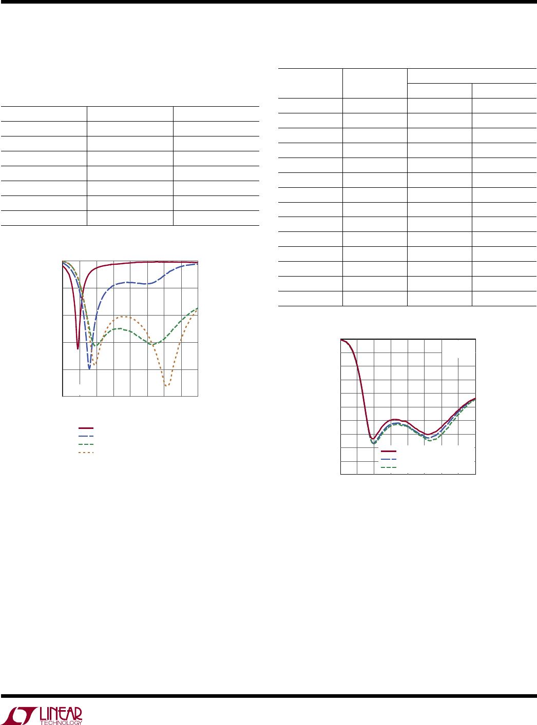
Figure 11. Conversion Gain and IF Output Return Loss vs
IF Frequency—Wideband Matching with 4:1 Transformer
Wideband IF Using Load Resistor and 4:1 Transformer
Wide IF bandwidth and high input 1dB compression can be
obtained by reducing the IF output resistance with a shunt
resistor (R3), as shown in Figure 10. This will reduce the
mixers conversion gain, but will not degrade the IIP3 or
noise figure. The evaluation board includes pads for R3
(and R4 for the B-channel). To accommodate the lower total
IF resistance, transformer T1 should be changed from an
8:1 impedance ratio to a 4:1 ratio. The value of the external
matching inductors L1 and L3 needs to be adjusted to ac
-
count for the differences in the IF transformer parasitics.
Table 5 summarizes the measured conversion gain, IIP3,
noise figure, RF input P1dB and IF bandwidth for three
values of load resistor
. Inductors L1 and L3 have been
increased from 180nH to 270nH to keep the IF match
centered at 190MHz (the 8:1 transformer has higher ca
-
pacitance). Also shown, for comparison, is the measured
performance using an 8:1 IF transformer and no load resis-
tor. Measured conversion gain and IF output return loss
versus IF frequency are shown for each case in Figure 11.
Table 5. Measured Performance Using IF Load Resistor (R3)
and 4:1 Transformer (RF = 1950MHz, Low-Side LO,
IF = 190MHz, V
CC
= 3.3V, T
C
= 25°C)
IF
XFMR R3 (Ω) G
C
(dB)
IIP3
(dBm)
SSB NF
(dB)
INPUT
P1dB
(dBm)
0.5dB IF
BANDWIDTH
(MHz)
8:1 2.0 26.8 11.7 10.2 –55/+85
4:1
1210 0.9 26.8 11.7 12.8 –90/+110
604 0.0 26.8 11.7 13.0 –100/+120
374 -1.1 26.8 11.8 13.3 –115/+120
IF FREQUENCY (MHz)
50
–1
0
2
170 250
5569 F11
–2
–3
90 130
210 290 330
–4
–5
1
5
15
35
–5
–15
–25
–35
25
CONVERSION GAIN (dB)
IF RETURN LOSS (dB)
8:1
1210Ω
604Ω
374Ω
374Ω
604Ω
1210Ω
8:1
1415
LTC5569
5569 F10
L1
L3
T1
4:1
C7
10nF
R3
V
CC
IFA
OUT
50Ω
IFA
+
IFA
V
CC
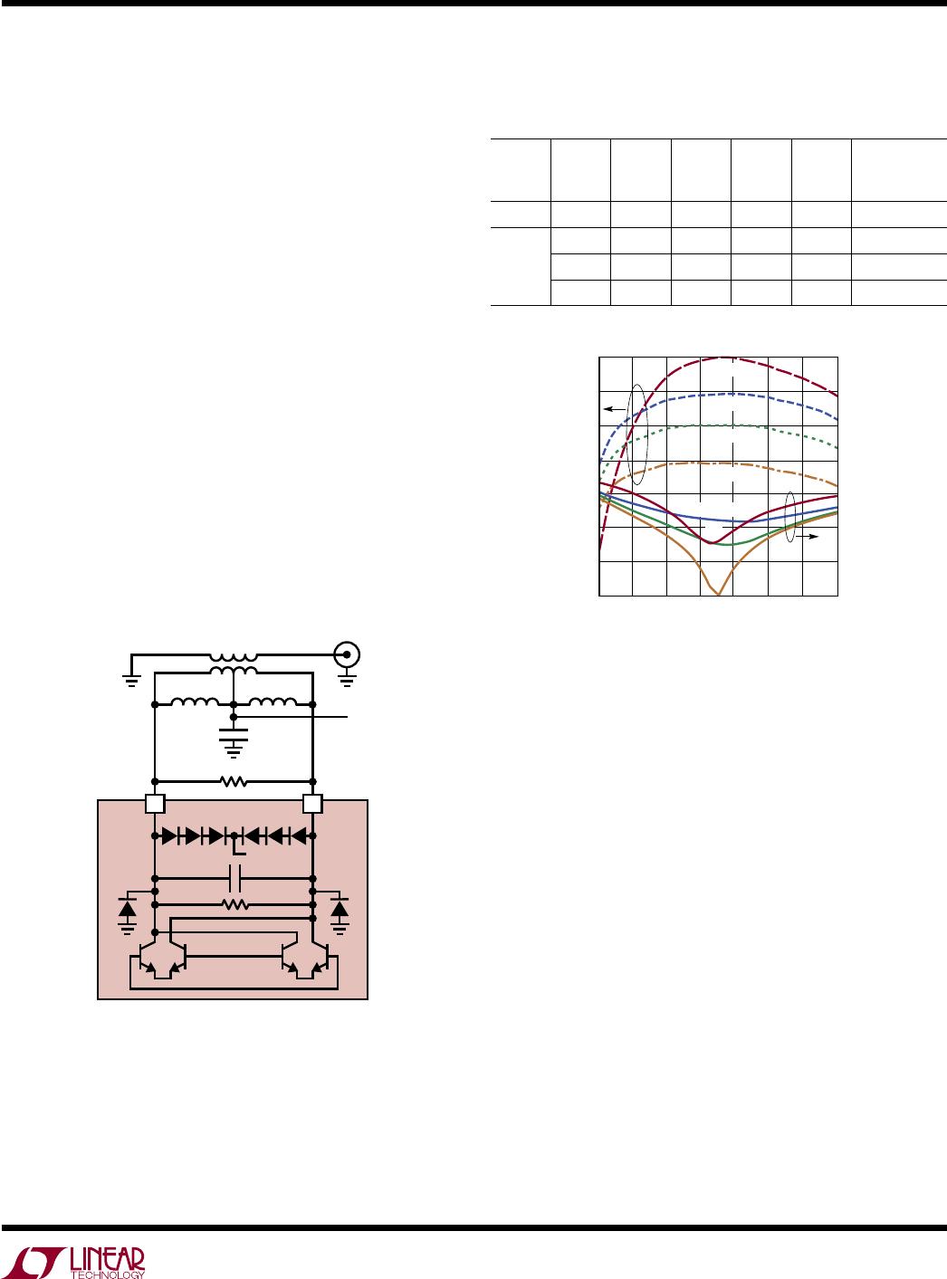
Figure 10. IF Output Schematic with Wideband Matching
and 4:1 Transformer
Discrete IF Balun Matching
For narrowband IF applications, it is possible to replace
the IF transformer with the discrete IF balun shown in
Figure 12 (only the A-channel is shown for clarity). The
values of L3, L7, C13 and C15 are calculated to realize a
180° phase shift at the desired IF frequency, and provide
a 50Ω single-ended output, using the equations listed
below. Inductor L1 is calculated to cancel the internal IF
capacitance (C
IF
from Table 4). L1 and L3 also supply DC
bias to the IF output pins. R5 and R7 are used to reduce
the differential output resistance (R
S
), which increases

LTC5569IUF#PBF

Mfr. #:
Manufacturer:
Analog Devices Inc.
Description:
RF Mixer 300MHz - 4GHz Dual Active Downconverting Mixer
Lifecycle:
New from this manufacturer.
Delivery:
DHL FedEx Ups TNT EMS
Payment:
T/T Paypal Visa MoneyGram Western Union

Products related to this Datasheet